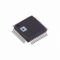
AD7612BSTZ-RL Analog Devices Inc, AD7612BSTZ-RL Datasheet - Page 5

AD7612BSTZ-RL
Manufacturer Part Number
AD7612BSTZ-RL
Description
IC,A/D CONVERTER,SINGLE,16-BIT,CMOS,QFP,48PIN
Manufacturer
Analog Devices Inc
Series
PulSAR®r
Datasheet
1.AD7612BSTZ.pdf
(32 pages)
Specifications of AD7612BSTZ-RL
Number Of Bits
16
Sampling Rate (per Second)
750k
Data Interface
Serial, Parallel
Number Of Converters
1
Power Dissipation (max)
230mW
Voltage Supply Source
Analog and Digital
Operating Temperature
-40°C ~ 85°C
Mounting Type
Surface Mount
Package / Case
48-LQFP
Lead Free Status / RoHS Status
Lead free / RoHS Compliant
For Use With
EVAL-AD7612CB - BOARD EVALUATION AD7612EVAL-AD7612CBZ - BOARD EVALUATION FOR AD7612
Lead Free Status / RoHS Status
Lead free / RoHS Compliant
Available stocks
Company
Part Number
Manufacturer
Quantity
Price
Company:
Part Number:
AD7612BSTZ-RL
Manufacturer:
Analog Devices Inc
Quantity:
10 000
TIMING SPECIFICATIONS
AVDD = DVDD = 5 V; OVDD = 2.7 V to 5.5 V; VCC = 15 V; VEE = −15 V; V
Table 3.
Parameter
CONVERSION AND RESET (See Figure 33 and Figure 34)
PARALLEL INTERFACE MODES (See Figure 35 and Figure 37)
MASTER SERIAL INTERFACE MODES
Convert Pulse Width
Time Between Conversions
CNVST Low to BUSY High Delay
BUSY High All Modes (Except Master Serial Read After Convert)
Aperture Delay
End of Conversion to BUSY Low Delay
Conversion Time
Acquisition Time
RESET Pulse Width
CNVST Low to DATA Valid Delay
DATA Valid to BUSY Low Delay
Bus Access Request to DATA Valid
Bus Relinquish Time
CS Low to SYNC Valid Delay
CS Low to Internal SDCLK Valid Delay
CS Low to SDOUT Delay
SDOUT Valid Setup Time
SDOUT Valid Hold Time
SDCLK Last Edge to SYNC Delay
CS High to SYNC HI-Z
CS High to Internal SDCLK HI-Z
CS High to SDOUT HI-Z
BUSY High in Master Serial Read After Convert
CNVST Low to SYNC Delay, Read After Convert
SYNC Deasserted to BUSY Low Delay
CNVST Low to SYNC Delay, Read During Convert
SYNC Asserted to SDCLK First Edge Delay
Internal SDCLK Period
Internal SDCLK High
Internal SDCLK Low
Warp Mode/Normal Mode/Impulse Mode
Warp Mode/Normal Mode/Impulse Mode
Warp Mode/Normal Mode/Impulse Mode
Warp Mode/Normal Mode/Impulse Mode
Warp Mode/Normal Mode/Impulse Mode
Warp Mode/Normal Mode/Impulse Mode
Warp Mode/Normal Mode/Impulse Mode
3
3
3
3
3
3
2
(See Figure 39 and Figure 40)
2
1
3
Rev. 0 | Page 5 of 32
Symbol
t
t
t
t
t
t
t
t
t
t
t
t
t
t
t
t
t
t
t
t
t
t
t
t
t
t
t
t
t
t
1
2
3
4
5
6
7
8
9
10
11
12
13
14
15
16
17
18
19
20
21
22
23
24
25
26
27
28
29
30
REF
= 5 V; all specifications T
Min
10
1.33/1.67/2
10
380
10
20
2
3
30
15
10
4
5
5
Typ
2
65/315/560
See Table 4
830/1070/1310
25
MIN
to T
MAX
, unless otherwise noted.
Max
35
950/1250/1450
950/1250/1450
910/1160/1410
40
15
10
10
10
45
10
10
10
AD7612
Unit
ns
μs
ns
ns
ns
ns
ns
ns
ns
ns
ns
ns
ns
ns
ns
ns
ns
ns
ns
ns
ns
ns
ns
ns
ns
ns
ns
ns
ns


