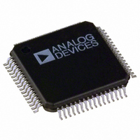
AD7656BSTZ-1 Analog Devices Inc, AD7656BSTZ-1 Datasheet - Page 6

AD7656BSTZ-1
Manufacturer Part Number
AD7656BSTZ-1
Description
6-CHANNEL 16-BIT SE BIPOLAR I.C.
Manufacturer
Analog Devices Inc
Specifications of AD7656BSTZ-1
Number Of Bits
16
Sampling Rate (per Second)
250k
Data Interface
Serial, Parallel
Number Of Converters
6
Power Dissipation (max)
143mW
Voltage Supply Source
Analog and Digital, Dual ±
Operating Temperature
-40°C ~ 85°C
Mounting Type
Surface Mount
Package / Case
64-LQFP
Lead Free Status / RoHS Status
Lead free / RoHS Compliant
For Use With
EVAL-AD7656-1EDZ - BOARD EVAL CONTROL AD7656-1EVAL-AD7656-1CBZ - BOARD EVAL FOR AD7656-1EVAL-AD7656CBZ - BOARD EVAL FOR AD7656
Lead Free Status / RoHS Status
Lead free / RoHS Compliant
Available stocks
Company
Part Number
Manufacturer
Quantity
Price
Company:
Part Number:
AD7656BSTZ-1
Manufacturer:
ADI
Quantity:
3
Company:
Part Number:
AD7656BSTZ-1
Manufacturer:
Analog Devices Inc
Quantity:
10 000
Part Number:
AD7656BSTZ-1
Manufacturer:
ADI/亚德诺
Quantity:
20 000
Company:
Part Number:
AD7656BSTZ-1-RL
Manufacturer:
Analog Devices Inc
Quantity:
10 000
AD7656-1/AD7657-1/AD7658-1
Parameter
LOGIC OUTPUTS
CONVERSION RATE
POWER REQUIREMENTS
1
2
3
4
The temperature range for the B version is −40°C to +85°C and for the Y version is −40°C to +125°C.
See the Terminology section.
Sample tested during initial release to ensure compliance.
Includes I
Output High Voltage (V
Output Low Voltage (V
Floating-State Leakage Current
Floating-State Output Capacitance
Output Coding
Conversion Time
Track-and-Hold Acquisition Time
Throughput Rate
V
V
AV
DV
V
I
I
I
Power Dissipation
TOTAL
SS
DD
DD
SS
DRIVE
Normal Mode—Static
Normal Mode—Operational
(Operational)
Partial Power-Down Mode
Full Power-Down Mode (STBY Pin)
Normal Mode—Static
Normal Mode—Operational
Partial Power-Down Mode
Full Power-Down Mode (STBY Pin)
CC
(Operational)
CC
4
AVCC
, I
VDD
, I
VSS
, I
VDRIVE
, and I
OL
OH
)
)
DVCC
.
2, 3
3
B Version
V
0.2
±10
10
3.1
550
250
5/15
−5/−15
5
5
3/5
18
26
0.25
0.25
7
400
94
140
40
25
DRIVE
Twos complement
− 0.2
1
Rev. 0 | Page 6 of 32
Y Version
V
0.2
±10
10
3.1
550
250
5/15
−5/−15
5
5
3/5
18
26
0.25
0.25
7
400
94
140
40
25
DRIVE
− 0.2
1
Unit
V min
V max
μA max
pF max
μs max
ns max
kSPS
V nom min/max
V nom min/max
V nom
V nom
V nom min/max
mA max
mA max
mA max
mA max
mA max
μA max
mW max
mW max
mW max
μW max
Parallel interface mode only
For the 4 × V
SCLK on or off, AV
Test Conditions/Comments
I
I
For the 4 × V
Digital inputs = 0 V or V
AV
V
f
V
V
V
AV
V
V
AV
V
f
SOURCE
SINK
SAMPLE
SAMPLE
SS
DD
SS
DD
SS
DD
SS
CC
CC
CC
= −16.5 V
= −16.5 V, f
= −16.5 V
= −16.5 V
= 200 μA
= 16.5 V, V
= 16.5 V, f
= 16.5 V, V
= DV
= DV
= DV
= 250 kSPS, AV
= 200 μA
= 250 kSPS
CC
CC
CC
= V
= V
= V
REF
REF
SAMPLE
SS
SS
SAMPLE
DRIVE
DRIVE
DRIVE
range, V
range, V
= −16.5 V
= −16.5 V
CC
= 250 kSPS
= 5.25 V, V
= 5.25 V, V
= 5.25 V, V
CC
= 250 kSPS
= DV
= DV
DD
DD
DRIVE
CC
= 10 V to 16.5 V
= −10 V to −16.5 V
CC
= V
= V
DD
DD
DD
DRIVE
DRIVE
= 16.5 V,
= 16.5 V,
= 16.5 V,
= 5.25 V,
= 5.25 V,


