AD7891AP-2 Analog Devices Inc, AD7891AP-2 Datasheet - Page 12
AD7891AP-2
Manufacturer Part Number
AD7891AP-2
Description
A/D Converter (A-D) IC
Manufacturer
Analog Devices Inc
Type
Data Acquisition System (DAS)r
Datasheet
1.AD7891BSZ-2.pdf
(20 pages)
Specifications of AD7891AP-2
No. Of Bits
12 Bit
Mounting Type
Surface Mount
Features
8?Ch., High?Speed, Data Acquisition System
No. Of Channels
8
Interface Type
Parallel
Package / Case
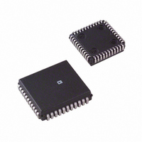
44-PLCC
Rohs Status
RoHS non-compliant
Resolution (bits)
12 b
Sampling Rate (per Second)
500k
Data Interface
Serial, Parallel
Voltage Supply Source
Single Supply
Voltage - Supply
5V
Operating Temperature
-40°C ~ 85°C
Lead Free Status / RoHS Status
Available stocks
Company
Part Number
Manufacturer
Quantity
Price
Company:

Part Number:
AD7891AP-2
Manufacturer:
Analog Devices Inc
Quantity:
10 000
Part Number:
AD7891AP-2
Manufacturer:
ADI/亚德诺
Quantity:
20 000
Company:
Part Number:
AD7891AP-2REEL
Manufacturer:
Analog Devices Inc
Quantity:
10 000


AD7891
CIRCUIT DESCRIPTION
Reference
The AD7891 contains a single reference pin labeled REF OUT/
REF IN that either provides access to the part’s own 2.5 V
internal reference or to which an external 2.5 V reference can be
connected to provide the reference source for the part. The part
is specified with a 2.5 V reference voltage. Errors in the reference
source result in gain errors in the transfer function of the AD7891
and add to the specified full-scale errors on the part. They also
result in an offset error injected into the attenuator stage.
The AD7891 contains an on-chip 2.5 V reference. To use this
reference as a reference source for the AD7891, simply connect
a 0.1 mF disc ceramic capacitor from the REF OUT/REF IN pin
to REFGND. REFGND should be connected to AGND or the
analog ground plane. The voltage that appears at the REF OUT/
REF IN pin is internally buffered before being applied to the
ADC. If this reference is required for use external to the AD7891,
it should be buffered since the part has a FET switch in series
with the reference, resulting in a source impedance for this
output of 2 kW nominal. The tolerance of the internal reference
is ± 10 mV at 25∞C with a typical temperature coefficient of
25 ppm/∞C and a maximum error over temperature of ± 20 mV.
If the application requires a reference with a tighter tolerance
or if the AD7891 needs to be used with a system reference, an
external reference can be connected to the REF OUT/REF IN
pin. The external reference overdrives the internal reference
and thus provides the reference source for the ADC. The refer-
ence input is buffered before being applied to the ADC and
the maximum input current is ± 100 mA. Suitable reference for
the AD7891 include the AD580, the AD680, the AD780, and
the REF43 precision 2.5 V references.
Analog Input Section
The AD7891 is offered as two part types: the AD7891-1 where
each input can be configured to have a ± 10 V or a ± 5 V input
range, and the AD7891-2 where each input can be configured
to have a 0 V to +2.5 V, 0 V to +5 V, and ± 2.5 V input range.
AD7891-1
Figure 5 shows the analog input section of the AD7891-1. Each
input can be configured for ± 5 V or ± 10 V operation. For 5 V
operation, the V
input voltage is applied to both. For ± 10 V operation, the V
input is tied to AGND and the input voltage is applied to the
V
fully interchangeable. Therefore, for ease of PCB layout on the
± 10 V range, the input voltage may be applied to the V
input while the V
INXA
input. The V
Figure 5. AD7891-1 Analog Input Structure
V
V
INXA
INXB
INXA
INXA
30k
30k
15k
INXA
and V
AGND
input is tied to AGND.
REFERENCE CIRCUITRY
and V
7.5k
INXB
TO
MULTIPLEXER
AD7891-1
TO ADC
INXB
inputs are tied together and the
inputs are symmetrical and
REF OUT/REF IN
REFERENCE
2.5V
2k
INXB
INXB
–12–
The input resistance for the ± 5 V range is typically 20 kW. For
the ± 10 V input range, the input resistance is typically 34.3 kW.
The resistor input stage is followed by the multiplexer, which is
followed by the high input impedance stage of the track/hold
amplifier.
The designed code transitions take place midway between suc-
cessive integer LSB values (i.e., 1/2 LSB, 3/2 LSBs, 5/2 LSBs).
LSB size is given by the formula 1 LSB = F
the ± 5 V range, 1 LSB = 10 V/4096 = 2.44 mV. For the ± 10 V
range, 1 LSB = 20 V/4096 = 4.88 mV. Output coding is deter-
mined by the FORMAT bit of the control register. The ideal
input/output code transitions are shown in Table I.
AD7891-2
Figure 6 shows the analog input section of the AD7891-2. Each
input can be configured for input ranges of 0 V to +5 V, 0 V to +2.5 V,
or ± 2.5 V. For the 0 V to 5 V input range, the V
tied to AGND and the input voltage is applied to the V
For the 0 V to 2.5 V input range, the V
are tied together and the input voltage is applied to both. For
the ± 2.5 V input range, the V
the input voltage is applied to the V
must have a low output impedance. If the internal reference on
the AD7891 is used, it must be buffered before being applied to
V
interchangeable. Therefore, for ease of PCB layout on the 0 V to +5 V
or ±2.5 V range, the input voltage may be applied to the V
input, while the V
The input resistance for both the 0 V to +5 V and ± 2.5 V ranges
is typically 3.6 kW. When an input is configured for 0 V to 2.5 V
operation, the input is fed into the high impedance stage of the
track/hold amplifier via the multiplexer and the two 1.8 kW
resistors in parallel.
The designed code transitions occur midway between successive
integer LSB values (i.e., 1/2 LSB, 3/2 LSBs, 5/2 LSBs). LSB size
is given by the formula 1 LSB = F
to 5 V range, 1 LSB = 5 V/4096 = 1.22 mV, for the 0 V to 2.5 V
range, 1 LSB = 2.5 V/4096 = 0.61 mV, and for the ± 2.5 V range,
1 LSB = 5 V/4096 = 1.22 mV. Output coding is determined by
the FORMAT bit in the control register. The ideal input/output
code transitions for the ± 2.5 V range are shown in Table I. The
ideal input/output code transitions for the 0 V to 5 V range and
the 0 V to 2.5 V range are shown in Table II.
INXB
. The V
Figure 6. AD7891-2 Analog Input Structure
V
V
INXB
INXA
INXA
1.8k
1.8k
INXA
and V
REFERENCE
CIRCUITRY
AGND
input is tied to AGND or 2.5 V.
TO ADC
INXB
TO
MULTIPLEXER
AD7891-2
inputs are symmetrical and fully
INXB
S
/4096. Therefore, for the 0 V
INXA
input is tied to 2.5 V and
INXA
REF OUT/REF IN
input. The 2.5 V source
REFERENCE
S
/4096. Therefore, for
and V
2.5V
2k
INXB
INXB
input is
INXA
inputs
INXB
REV. D
input.
Related parts for AD7891AP-2
Image
Part Number
Description
Manufacturer
Datasheet
Request
R

Part Number:
Description:
RF/COAXIAL ADAPTER, TRB JACK-TRB JACK
Manufacturer:
TROMPETER ELECTRONICS
Datasheet:

Part Number:
Description:
±1.7g Dual-Axis IMEMS Accelerometer Evaluation Board
Manufacturer:
Analog Devices Inc
Datasheet:

Part Number:
Description:
Inertial Sensor Evaluation System
Manufacturer:
Analog Devices Inc
Datasheet:
Part Number:
Description:
Manufacturer:
Analog Devices Inc
Datasheet:
Part Number:
Description:
Manufacturer:
Analog Devices Inc
Datasheet:
Part Number:
Description:
Manufacturer:
Analog Devices Inc
Datasheet:
Part Number:
Description:
Manufacturer:
Analog Devices Inc
Datasheet:
Part Number:
Description:
Manufacturer:
Analog Devices Inc
Datasheet:
Part Number:
Description:
Manufacturer:
Analog Devices Inc
Datasheet:
Part Number:
Description:
Manufacturer:
Analog Devices Inc
Datasheet:
Part Number:
Description:
Manufacturer:
Analog Devices Inc
Datasheet:
Part Number:
Description:
Manufacturer:
Analog Devices Inc
Datasheet:
Part Number:
Description:
Manufacturer:
Analog Devices Inc
Datasheet: