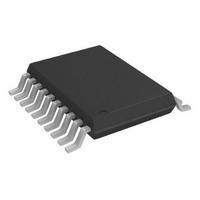
AD7998BRU-0 Analog Devices Inc, AD7998BRU-0 Datasheet - Page 22

AD7998BRU-0
Manufacturer Part Number
AD7998BRU-0
Description
IC,Data Acquisition System,8-CHANNEL,12-BIT,TSSOP,20PIN,PLASTIC
Manufacturer
Analog Devices Inc
Datasheet
1.AD7997BRUZ-1.pdf
(32 pages)
Specifications of AD7998BRU-0
Number Of Bits
12
Sampling Rate (per Second)
188k
Data Interface
I²C, Serial
Number Of Converters
1
Power Dissipation (max)
2.2mW
Voltage Supply Source
Single Supply
Operating Temperature
-40°C ~ 85°C
Mounting Type
Surface Mount
Package / Case
20-TSSOP (0.173", 4.40mm Width)
Lead Free Status / RoHS Status
Contains lead / RoHS non-compliant
For Use With
EVAL-AD7998CBZ - BOARD EVALUATION FOR AD7998CBZ
Lead Free Status / RoHS Status
Contains lead / RoHS non-compliant, Contains lead / RoHS non-compliant
AD7997/AD7998
CYCLE TIMER REGISTER
The cycle timer register is an 8-bit, read/write register that
stores the conversion interval value for the automatic cycle
interval mode of the AD7997/AD7998 (see the Modes of
Operation section). D5 to D3 of the cycle timer register are
unused and should contain 0s at all times. On power-up, the
cycle timer register contains all 0s, thus disabling automatic
cycle operation of the AD7997/AD7998. To enable automatic
cycle mode, the user must write to the cycle timer register,
selecting the required conversion interval by programming Bits
D2 to D0. Table 23 shows the structure of the cycle timer
register, while Table 24 shows how the bits in this register are
decoded to provide various automatic sampling intervals.
Table 23. Cycle Timer Register and Defaults at Power-Up
D7
Sample
Delay
0
Table 24. Cycle Timer Intervals
D2
0
0
0
0
1
1
1
1
D1
0
0
1
1
0
0
1
1
D6
Bit Trial
Delay
0
D0
0
1
0
1
0
1
0
1
D5
0
0
Typical Conversion Interval
(T
Mode Not Selected
T
T
T
T
T
T
T
CONVERT
CONVERT
CONVERT
CONVERT
CONVERT
CONVERT
CONVERT
D4
0
0
CONVERT
× 32
× 64
× 128
× 256
× 512
× 1024
× 2048
D3
0
0
= Conversion Time)
D2
Cyc
Bit2
0
D1
Cyc
Bit1
0
D0
Cyc
Bit0
0
Rev. 0 | Page 22 of 32
SAMPLE DELAY AND BIT TRIAL DELAY
It is recommended that no I
conversion is taking place. However, if this is not possible, for
example when operating in Mode 2 or Mode 3, then in order to
maintain the performance of the ADC, Bits D7 and D6 in the
cycle timer register are used to delay critical sample intervals
and bit trials from occurring while there is activity on the I
bus. This results in a quiet period for each bit decision. In
certain cases where there is excessive activity on the interface
lines, this may have the effect of increasing the overall
conversion time. However, if bit trial delays extend longer than
1 µs, the conversion terminates.
When Bits D7 and D6 are both 0, the bit trial and sample
interval delaying mechanism is implemented. The default
setting of D7 and D6 is 0. To turn off both delay mechanisms,
set D7 and D6 to 1.
Table 25. Cycle Timer Register and Defaults at Power-up
D7
Sample
Delay
0
D6
Bit Trial
Delay
0
D5
0
0
2
C bus activity occurs when a
D4
0
0
D3
0
0
D2
Cyc
Bit 2
0
D1
Cyc
Bit 1
0
D0
Cyc
Bit 0
0
2
C


