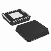
AD8193ACPZ-R7 Analog Devices Inc, AD8193ACPZ-R7 Datasheet - Page 14

AD8193ACPZ-R7
Manufacturer Part Number
AD8193ACPZ-R7
Description
IC,Telecom Switching Circuit,LLCC,32PIN,PLASTIC
Manufacturer
Analog Devices Inc
Datasheet
1.AD8193ACPZ-R7.pdf
(16 pages)
Specifications of AD8193ACPZ-R7
Function
Switch
Circuit
1 x 2:1
Voltage Supply Source
Single Supply
Voltage - Supply, Single/dual (±)
3 V ~ 3.6 V
Current - Supply
50mA
Operating Temperature
-40°C ~ 85°C
Mounting Type
Surface Mount
Package / Case
32-LFCSP
Lead Free Status / RoHS Status
Lead free / RoHS Compliant
AD8193
Evaluation Board
The AD8193 evaluation board illustrates one way to implement
a 2:1 HDMI link switch with an AD8193 and a CMOS switch.
The AD8193 evaluation board deviates from a typical applica-
tion in that it uses an HDMI connector for the output as well as
for the inputs. This setup makes it easy to connect equipment to
the AD8193 evaluation board with standard HDMI cables.
CONNECTOR
CONNECTOR
Figure 24. Block Diagram of AD8193 Evaluation Board Showing Output Crossover
CONNECTOR
HDMI
HDMI
HDMI
Figure 25. HDMI Signals to HDMI Receiver, No Crossover Required
19
1
19
1
19
1
Rev. 0 | Page 14 of 16
AD8193
AD8193
However, this arrangement requires crossing over the TMDS
signals on the output side (see Figure 24).
In a typical application, the output of the AD8193 is routed
directly into an HDMI receiver. Because a receiver is generally
designed to interface directly to an HDMI input connector, it is
not necessary to cross over the TMDS signals in a typical
application (see Figure 25).
CROSSOVER
REQUIRED
19
1
RECEIVER
CONNECTOR
HDMI
HDMI


