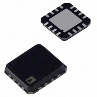
AD8222BCPZ-RL Analog Devices Inc, AD8222BCPZ-RL Datasheet

AD8222BCPZ-RL
Specifications of AD8222BCPZ-RL
Related parts for AD8222BCPZ-RL
AD8222BCPZ-RL Summary of contents
Page 1
FEATURES Two channels in small 4 mm × LFCSP Gain set with 1 resistor per amplifier ( 10,000) Low noise 8 nV/√ kHz 0.25 μV p-p (0 Hz) High accuracy ...
Page 2
AD8222 TABLE OF CONTENTS Features .............................................................................................. 1 Applications ....................................................................................... 1 Functional Block Diagram .............................................................. 1 General Description ......................................................................... 1 Revision History ............................................................................... 2 Specifications ..................................................................................... 3 Absolute Maximum Ratings ............................................................ 6 Thermal Resistance ...................................................................... 6 ESD Caution .................................................................................. 6 Pin ...
Page 3
SPECIFICATIONS V = ± 25° REF A Table 2. Single-Ended and Differential Parameter Conditions COMMON-MODE REJECTION V CM RATIO (CMRR) CMRR kΩ source ...
Page 4
AD8222 Parameter Conditions REFERENCE INPUT +IN Voltage Range Reference Gain to Output Reference Gain Error GAIN (49.4 kΩ/R Gain Range Gain Error V OUT ...
Page 5
V = ± 25° kΩ, unless otherwise noted. S REF A L Table 3. Single-Ended Output Configuration—Dynamic Performance (Both Amplifiers) Parameter DYNAMIC RESPONSE Small Signal −3 dB Bandwidth G = ...
Page 6
AD8222 ABSOLUTE MAXIMUM RATINGS Table 5. Parameter Supply Voltage Output Short-Circuit Current Duration Input Voltage (Common Mode) Differential Input Voltage Storage Temperature Range Operational Temperature Range Package Glass Transition Temperature (T ESD Human Body Model Charge Device Model Stresses above ...
Page 7
PIN CONFIGURATION AND FUNCTION DESCRIPTIONS Table 7. Pin Function Descriptions Pin No Mnemonic 1 −IN1 2 RG1 3 RG1 4 +IN1 REF1 7 REF2 8 − +IN2 10 RG2 11 RG2 12 −IN2 13 ...
Page 8
AD8222 TYPICAL PERFORMANCE CHARACTERISTICS 500 400 300 200 100 0 –50 –40 –30 –20 – CMRR (µV/V) Figure 3. Typical Distribution for CMRR ( 300 250 200 150 100 10 0 –100 ...
Page 9
V = ±15V S 100 ±5V S –50 –100 –150 –200 –15 –10 – COMMON-MODE VOLTAGE (V) Figure 9. I vs. Common-Mode Voltage BIAS 2.0 1.8 1.6 1.4 1.2 1.0 0.8 0.6 ...
Page 10
AD8222 70 GAIN = 1000 60 50 GAIN = 100 40 30 GAIN = GAIN = 1 0 –10 –20 –30 –40 100 1k 10k 100k FREQUENCY (Hz) Figure 15. Gain vs. Frequency 160 GAIN = 1000 ...
Page 11
LOAD RESISTANCE (Ω) Figure 21. Output Voltage Swing vs. Load Resistance +V –0 S –1 SOURCING –2 – SINKING +1 – ...
Page 12
AD8222 0.1µV/DIV Figure 27. 0 RTI Voltage Noise (G = 1000) 1k 100 100 1k FREQUENCY (Hz) Figure 28. Current Noise Spectral Density vs. Frequency 5pA/DIV Figure 29. 0 ...
Page 13
TO 0.01% 16.2µs TO 0.001% 0.002%/DIV Figure 33. Large Signal Pulse Response and Settling Time (G = 100) 5V/DIV 83µs TO 0.01% 112µs TO 0.001% 0.002%/DIV Figure 34. Large Signal Pulse Response and Settling Time (G = 1000) ...
Page 14
AD8222 15 10 SETTLED TO 0.001% SETTLED TO 0.01 OUTPUT VOLTAGE STEP SIZE (V) Figure 39. Settling Time vs. Step Size ( 100 SETTLED TO 0.001% 10 SETTLED TO 0.01 ...
Page 15
THEORY OF OPERATION I I COMPENSATION 400Ω –IN Q1 –V S AMPLIFIER ARCHITECTURE The two instrumentation amplifiers of the AD8222 are based on the classic 3-op-amp topology. Figure 44 shows a simplified schematic of one of ...
Page 16
AD8222 REFERENCE TERMINAL The output voltage of an AD8222 channel is developed with respect to the potential on the corresponding reference terminal. Typically the reference terminal is connected to ground, but it can also be driven with a voltage to ...
Page 17
The AD8222 should be decoupled with 0.1 μF bypass capacitors, one for each supply. The positive supply decoupling capacitor should be placed near Pin 16, and the negative supply ...
Page 18
AD8222 INPUT PROTECTION All terminals of the AD8222 are protected against ESD (1 kV, human body model). In addition, the input structure allows for dc overload conditions of about 2.5 V beyond the supplies. Input Voltages Beyond the Rails For ...
Page 19
APPLICATIONS INFORMATION DIFFERENTIAL OUTPUT The differential configuration of the AD8222 has the same excellent dc precision specifications as the single-ended output configuration and is recommended for applications in the frequency range 100 kHz. The circuit configuration is ...
Page 20
AD8222 + 10µF 0.1µF 100pF NPO 1kΩ 5% +IN 1000pF 1kΩ –IN 100pF NPO 5% 10µF 0.1µF + DRIVING A DIFFERENTIAL INPUT ADC The AD8222 can be configured in differential output mode to drive a differential analog-to-digital converter. Figure 51 ...
Page 21
DRIVING CABLING All cables have a certain capacitance per unit length, which varies widely with cable type. The capacitive load from the cable may cause peaking in the AD8222’s output response. To reduce the peaking, use a resistor between the ...
Page 22
AD8222 OUTLINE DIMENSIONS PIN 1 INDICATOR 12° MAX 1.00 0.85 0.80 SEATING PLANE PIN 1 INDICATOR 1.00 0.85 0.80 SEATING PLANE 4.00 0.60 MAX BSC 3.75 EXPOSED BSC SQ PAD 0. BSC TOP VIEW 1.95 ...
Page 23
... AD8222ACPZ-R7 −40°C to +85°C AD8222ACPZ-RL −40°C to +85°C AD8222ACPZ-WP −40°C to +85°C AD8222BCPZ-R7 −40°C to +85°C AD8222BCPZ-RL −40°C to +85°C AD8222BCPZ-WP −40°C to +85°C AD8222HACPZ-R7 −40°C to +85°C AD8222HACPZ-RL −40°C to +85°C AD8222HACPZ-WP − ...
Page 24
AD8222 NOTES ©2006–2010 Analog Devices, Inc. All rights reserved. Trademarks and registered trademarks are the property of their respective owners. D05947-0-2/10(A) Rev Page ...


