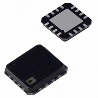
AD8222BCPZ-RL Analog Devices Inc, AD8222BCPZ-RL Datasheet - Page 18

AD8222BCPZ-RL
Manufacturer Part Number
AD8222BCPZ-RL
Description
IC,Instrumentation Amplifier,DUAL,LLCC,16PIN,PLASTIC
Manufacturer
Analog Devices Inc
Datasheet
1.AD8222BCPZ-R7.pdf
(24 pages)
Specifications of AD8222BCPZ-RL
Amplifier Type
Instrumentation
Number Of Circuits
2
Slew Rate
2 V/µs
-3db Bandwidth
1.2MHz
Current - Input Bias
200pA
Voltage - Input Offset
60µV
Current - Supply
900µA
Current - Output / Channel
18mA
Voltage - Supply, Single/dual (±)
4.6 V ~ 36 V, ±2.3 V ~ 18 V
Operating Temperature
-40°C ~ 85°C
Mounting Type
Surface Mount
Package / Case
16-LFCSP
Lead Free Status / RoHS Status
Lead free / RoHS Compliant
Output Type
-
Gain Bandwidth Product
-
Lead Free Status / RoHS Status
Lead free / RoHS Compliant
AD8222
INPUT PROTECTION
All terminals of the AD8222 are protected against ESD (1 kV,
human body model). In addition, the input structure allows for
dc overload conditions of about 2.5 V beyond the supplies.
Input Voltages Beyond the Rails
For larger input voltages, an external resistor should be used in
series with each input to limit current during overload conditions.
The AD8222 can safely handle a continuous 6 mA current. The
limiting resistor can be computed from
For applications in which the AD8222 encounters extreme over-
load voltages, such as cardiac defibrillators, external series
resistors and low leakage diode clamps, such as the BAV199L,
the FJH1100, or the SP720, should be used.
Differential Input Voltages at High Gains
When operating at high gain, large differential input voltages
can cause more than 6 mA of current to flow into the inputs.
This condition occurs when the differential voltage exceeds
the following critical voltage:
This is true for differential voltages of either polarity.
The maximum allowed differential voltage can be increased by
adding an input protection resistor in series with each input.
The value of each protection resistor should be
RF INTERFERENCE
RF rectification is often a problem when amplifiers are used in
applications where there are strong RF signals. The disturbance
can appear as a small dc offset voltage. High frequency signals
can be filtered with a low-pass, RC network placed at the input
of the instrumentation amplifier, as shown in Figure 48. The
filter limits the input signal bandwidth according to the
following relationship:
where C
V
R
R
FilterFreq
FilterFreq
PROTECT
CRITICAL
LIMIT
D
≥ 10C
= (V
= (400 + R
V
Diff
CM
IN
C
.
DIFF_MAX
6
mA
V
2
2
SUPPLY
R
R
G
1
) × (6 mA)
(2
− V
C
C
1
D
C
CRITICAL
400
C
C
Ω
)
)/6 mA
Rev. A | Page 18 of 24
Figure 48 shows an example where the differential filter fre-
quency is approximately 2 kHz, and the common-mode filter
frequency is approximately 40 kHz.
Values of R and C
between the R × C
negative input degrades the CMRR of the AD8222. By using a
value of C
mismatch is reduced and performance is improved.
COMMON-MODE INPUT VOLTAGE RANGE
The 3-op-amp architecture of the AD8222 applies gain and then
removes the common-mode voltage. Therefore, internal nodes
in the AD8222 experience a combination of both the gained
signal and the common-mode signal. This combined signal can
be limited by the voltage supplies even when the individual
input and output signals are not. Figure 7 and Figure 8 show the
allowable common-mode input voltage ranges for various
output voltages, supply voltages, and gains.
D
4.02kΩ
4.02kΩ
10× larger than the value of C
R
R
C
should be chosen to minimize RFI. Mismatch
C
at the positive input and the R × C
C
1nF
C
10nF
C
1nF
Figure 48. RFI Suppression
C
D
C
499Ω
R1
0.1µF
0.1µF
+IN
–IN
+15V
AD8222
–15V
C
REF
, the effect of the
10µF
10µF
V
OUT
C
at


