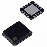
AD8231ACPZ-RL Analog Devices Inc, AD8231ACPZ-RL Datasheet - Page 19

AD8231ACPZ-RL
Manufacturer Part Number
AD8231ACPZ-RL
Description
IC,Instrumentation Amplifier,SINGLE,LLCC,16PIN,PLASTIC
Manufacturer
Analog Devices Inc
Datasheet
1.AD8231-EVALZ.pdf
(24 pages)
Specifications of AD8231ACPZ-RL
Amplifier Type
Instrumentation
Number Of Circuits
2
Output Type
Rail-to-Rail
Slew Rate
1.1 V/µs
Gain Bandwidth Product
7MHz
Current - Input Bias
250pA
Voltage - Input Offset
4µV
Current - Supply
4mA
Current - Output / Channel
70mA
Voltage - Supply, Single/dual (±)
3 V ~ 6 V, ±1.5 V ~ 3 V
Operating Temperature
-40°C ~ 125°C
Mounting Type
Surface Mount
Package / Case
16-LFCSP
Lead Free Status / RoHS Status
Lead free / RoHS Compliant
For Use With
AD8231-EVALZ - BOARD EVAL FOR AD8231
-3db Bandwidth
-
Lead Free Status / RoHS Status
Lead free / RoHS Compliant
LAYOUT
The AD8231 is a high precision device. To ensure optimum
performance at the PCB level, care must be taken in the design
of the board layout. The AD8231 pinout is arranged in a logical
manner to aid in this task.
Power Supplies
The AD8231 should be decoupled with a 0.1 μF bypass capacitor
between the two supplies. This capacitor should be placed as close
as possible to Pin 11 and Pin 12, either directly next to the pins or
beneath the pins on the backside of the board. The auto-zero
architecture of the AD8231 requires a low ac impedance between
the supplies. Long trace lengths to the bypass capacitor increase
this impedance, which results in a larger input offset voltage.
A stable dc voltage should be used to power the instrumentation
amplifier. Noise on the supply pins can adversely affect
performance.
Package Considerations
The AD8231 comes in a 4 mm × 4 mm LFCSP. Beware of
blindly copying the footprint from another 4 mm × 4 mm
LFCSP part; it cannot have the same thermal pad size and leads.
Refer to the Outline Dimensions section to verify that
the PCB symbol has the correct dimensions. Space between
the leads and thermal pad should be kept as wide as possible
for the best bias current performance.
Thermal Pad
The AD8231 4 mm × 4 mm LFCSP comes with a thermal pad.
This pad is connected internally to −V
left unconnected or connected to the negative supply rail. For
high vibration applications, a landing is recommended.
Because the AD8231 dissipates little power, heat dissipation
is rarely an issue. If improved heat dissipation is desired (for
example, when ambient temperatures are near 125°C or when
driving heavy loads), connect the thermal pad to the negative
supply rail. For the best heat dissipation performance, the
negative supply rail should be a plane in the board. See the
Thermal Resistance section for thermal coefficients with and
without the pad soldered.
INPUT BIAS CURRENT RETURN PATH
The input bias current of the AD8231 must have a return path
to common. When the source, such as a thermocouple, cannot
provide a return current path, one should be created, as shown
in Figure 51.
S
. The pad can either be
Rev. A | Page 19 of 24
INPUT PROTECTION
All terminals of the AD8231 are protected against ESD. In
addition, the input structure allows for dc overload conditions
a diode drop above the positive supply and a diode drop below
the negative supply. Voltages beyond these limits cause the ESD
diodes to conduct and current to flow. If overvoltage events are
anticipated, an external resistor should be used in series with
each of the inputs to limit the current to below 10 mA. Currents
up to 100 mA can be sustained for a few seconds.
Note that if either input is brought below the negative supply
to the point where the ESD diode turns on, the AD8231 output
can phase-reverse.
CAPACITIVELY COUPLED
C
C
THERMOCOUPLE
TRANSFORMER
INCORRECT
AD8231
+V
–V
AD8231
AD8231
+V
–V
+V
–V
S
S
S
S
S
S
REF
Figure 51. Creating an I
REF
REF
f
HIGH-PASS
=
CAPACITIVELY COUPLED
2πRC
1
10MΩ
BIAS
C
C
Path
THERMOCOUPLE
R
R
TRANSFORMER
CORRECT
AD8231
AD8231
AD8231
+V
–V
+V
–V
+V
–V
AD8231
S
S
S
S
S
S
REF
REF
REF


