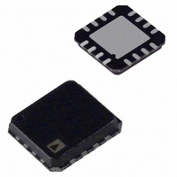
AD8295ACPZ-RL Analog Devices Inc, AD8295ACPZ-RL Datasheet

AD8295ACPZ-RL
Specifications of AD8295ACPZ-RL
Related parts for AD8295ACPZ-RL
AD8295ACPZ-RL Summary of contents
Page 1
FEATURES Saves board space Includes precision in-amp amps, and 2 matched resistors 4 mm × LFCSP No heat slug for more routing room Differential output fully specified In-amp specifications Gain set with 1 external resistor (gain ...
Page 2
AD8295 TABLE OF CONTENTS Features .............................................................................................. 1 Applications ....................................................................................... 1 Connection Diagram ....................................................................... 1 General Description ......................................................................... 1 Revision History ............................................................................... 2 Specifications ..................................................................................... 3 Instrumentation Amplifier Specifications, Single-Ended and Differential Output Configurations ........................................... 3 Op Amp Specifications ................................................................ 5 ...
Page 3
SPECIFICATIONS INSTRUMENTATION AMPLIFIER SPECIFICATIONS, SINGLE-ENDED AND DIFFERENTIAL OUTPUT CONFIGURATIONS V = ± 25° REF A Table 2. Parameter Test Conditions COMMON-MODE REJECTION V CM RATIO (CMRR) CMRR, DC ...
Page 4
AD8295 Parameter Test Conditions GAIN (49.4 kΩ/R Gain Range Gain Error V OUT 100 G = 1000 Gain Nonlinearity V OUT ...
Page 5
Parameter Test Conditions INPUT Input Impedance Differential Common Mode 1 Input Operating Voltage Range V S Over Temperature Input Operating Voltage Range V S Over Temperature T A OUTPUT R L Output Swing V S Over Temperature ...
Page 6
AD8295 INTERNAL RESISTOR NETWORK When used with internal Op Amp A1, T Table 4. Parameter Nominal Resistor Value Resistor Matching Matching Temperature Coefficient Absolute Resistor Accuracy Absolute Temperature Coefficient POWER AND TEMPERATURE SPECIFICATIONS V = ± ...
Page 7
ABSOLUTE MAXIMUM RATINGS Table 6. Parameter Supply Voltage Output Short-Circuit Current Input Voltage Common-Mode Differential Storage Temperature Range 1 Operating Temperature Range Lead Temperature (Soldering, 10 sec) Junction Temperature ESD (Human Body Model) ESD (Charged Device Model) ESD (Machine Model) ...
Page 8
AD8295 PIN CONFIGURATION AND FUNCTION DESCRIPTIONS Table 8. Pin Function Descriptions Pin No. Mnemonic Description 1 −IN In-Amp Negative Input In-Amp Gain-Setting Resistor Terminals +IN In-Amp Positive Input. 5 −V Negative Supply REF ...
Page 9
TYPICAL PERFORMANCE CHARACTERISTICS IN-AMP V = ± 25° kΩ, unless otherwise noted. S REF A L 800 600 400 200 0 –100 –50 0 CMRR (µV/V) Figure 3. Typical Distribution ...
Page 10
AD8295 –1 –2 –3 –4 –5 –4 –3 –2 – OUTPUT VOLTAGE (V) Figure 9. Input Common-Mode Voltage Range vs. Output Voltage 100 ±2.5 V, ± ...
Page 11
GAIN = 1000 140 GAIN = 100 GAIN = 10 120 GAIN = 1 100 0 100 1k 10k FREQUENCY (Hz) Figure 15. Negative PSRR vs. Frequency, RTI ...
Page 12
AD8295 +V – –0 10kΩ L –0.8 –1.2 –1.6 +1.6 +1.2 +0 10kΩ L +0.4 – SUPPLY VOLTAGE (V) Figure 21. Output Voltage Swing vs. Supply Voltage, G ...
Page 13
Figure 27. 0 RTI Voltage Noise 0.1µV/DIV Figure 28. 0 RTI Voltage Noise 1000 1k 100 100 1k FREQUENCY (Hz) Figure 29. Current ...
Page 14
AD8295 5V/DIV 4.8µs TO 0.01% 6.6µs TO 0.001% 0.002%/DIV Figure 33. Large Signal Pulse Response and Settling Time 5V/DIV 9.2µs TO 0.01% 16.2µs TO 0.001% 0.002%/DIV Figure 34. Large Signal Pulse Response and Settling Time ...
Page 15
Figure 39. Small Signal Pulse Response 1000 SETTLED TO 0.001% SETTLED TO 0.01 OUTPUT VOLTAGE STEP SIZE (V) Figure 40. Settling Time vs. Output Voltage Step Size ...
Page 16
AD8295 OP AMPS V = ± 25° kΩ, Op Amp A1 and Op Amp A2, unless otherwise noted 100 80 OPEN-LOOP GAIN 60 PHASE –20 –40 10 100 ...
Page 17
TIME (Sec) Figure 48. 0 Noise 1k 100 100 1k FREQUENCY (Hz) Figure 49. Current Noise Density ...
Page 18
AD8295 SYSTEM V = ± 25°C, unless otherwise noted. S REF A 170 GAIN = 1000 150 130 GAIN = 1 110 100 1k 10k FREQUENCY (Hz) Figure 53. ...
Page 19
THEORY OF OPERATION As shown in Figure 58, the AD8295 contains a precision instrumentation amplifier, two uncommitted op amps, and a precision resistor array. These components allow many common applications to be wired using simple pin-strapping, directly at the IC. ...
Page 20
AD8295 Reference Terminal The output voltage of the AD8295 instrumentation amplifier is developed with respect to the potential on the reference terminal (REF). This is useful when the output signal needs to be offset to a precise dc level. The ...
Page 21
Power Supplies A stable dc voltage should be used to power the instrumentation amplifier. Noise on the supply pins can adversely affect perfor- mance. See the PSRR performance curves in Figure 14 and Figure 15 for more information. A 0.1 ...
Page 22
AD8295 +V S 0.1µF C 1nF C R +IN 4.02kΩ AD8295 10nF D IN-AMP R –IN 4.02kΩ C 1nF C 0.1µF –V S Figure 63. RFI Suppression Lower cutoff frequencies improve RFI robustness. Accuracy of the C ...
Page 23
APPLICATIONS INFORMATION CREATING A REFERENCE VOLTAGE AT MIDSCALE A reference voltage other than ground is often useful, for example, when driving a single-supply ADC. Creating a reference voltage derived from a voltage divider is straight- forward with the AD8295 (see ...
Page 24
AD8295 TWO-POLE SALLEN-KEY FILTER Figure 69 shows the in-amp output section of the AD8295 being low-pass filtered using a two-pole Sallen-Key filter. The filter section consists of Op Amp A2, External Resistors R1 and R2, as well as Capacitors C1 ...
Page 25
DRIVING DIFFERENTIAL ADCs Figure 71 shows how to configure the AD8295 to drive a differ- ential ADC. The circuit shown uses very little board space and consumes little power. With the AD7690, this configuration gives excellent dc performance and a ...
Page 26
... INDICATOR 1.00 0.85 0.80 SEATING PLANE ORDERING GUIDE Model Temperature Range 1 AD8295ACPZ-R7 −40°C to +85°C 1 AD8295ACPZ-RL −40°C to +85°C AD8295ACPZ-WP 1 −40°C to +85°C 1 AD8295BCPZ-R7 −40°C to +85°C 1 AD8295BCPZ-RL −40°C to +85°C 1 AD8295BCPZ-WP −40°C to +85° RoHS Compliant Part ...
Page 27
NOTES Rev Page AD8295 ...
Page 28
AD8295 NOTES ©2008–2009 Analog Devices, Inc. All rights reserved. Trademarks and registered trademarks are the property of their respective owners. D07343-0-6/09(A) Rev Page ...


