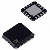
AD8295ACPZ-RL Analog Devices Inc, AD8295ACPZ-RL Datasheet - Page 22

AD8295ACPZ-RL
Manufacturer Part Number
AD8295ACPZ-RL
Description
Dual Precision InAmp
Manufacturer
Analog Devices Inc
Datasheet
1.AD8295ACPZ-R7.pdf
(28 pages)
Specifications of AD8295ACPZ-RL
Amplifier Type
Instrumentation
Number Of Circuits
3
Slew Rate
2 V/µs
Gain Bandwidth Product
1MHz
-3db Bandwidth
1.2MHz
Current - Input Bias
500pA
Voltage - Input Offset
120µV
Current - Supply
2mA
Current - Output / Channel
18mA
Voltage - Supply, Single/dual (±)
4.6 V ~ 36 V, ±2.3 V ~ 18 V
Operating Temperature
-40°C ~ 85°C
Mounting Type
Surface Mount
Package / Case
16-LFCSP
Lead Free Status / RoHS Status
Lead free / RoHS Compliant
Output Type
-
Lead Free Status / RoHS Status
Lead free / RoHS Compliant
AD8295
Lower cutoff frequencies improve RFI robustness. Accuracy of
the C
the R × C
input degrades the CMRR of the AD8295. Keeping C
10 times larger than C
DIFFERENTIAL OUTPUT
The AD8295 can be pin-strapped to provide a differential
output; the simplified schematic is shown in Figure 64 and the
full pin connection is shown in Figure 65. This configuration
uses the instrumentation amplifier to maintain the differential
voltage, while the op amp maintains the common-mode voltage.
Because the in-amp precisely controls the output relative to its
reference pin, this circuit has the same excellent dc performance
as the single-ended output configuration. The transfer function
for the differential and common-mode outputs are as follows:
where:
This configuration is fully specified (see Table 2, Figure 55, and
Figure 56). DC performance is the same as for the single-ended
configuration; ac performance is slightly different.
V
V
G
C
Figure 64. Differential Output Configuration Using an Op Amp
DIFF_OUT
CM_OUT
capacitors is important, because any mismatch between
=
1 +
C
+IN
–IN
at the positive input and the R × C
4.02kΩ
4.02kΩ
= (V
49
R
R
= V
4 .
R
C
C
C
G
–
+
OUT+
OUT+
C
D
C
kΩ
IN-AMP
REF
Figure 63. RFI Suppression
1nF
10nF
1nF
− V
+ V
C
is recommended.
OUT−
OUT−
20kΩ
20kΩ
R
G
0.1µF
0.1µF
)/2 = V
+IN
= G × (V
–IN
AD8295
+V
IN-AMP
–V
–
REF
S
S
V
IN+
A1
REF
− V
+
INPUT
REF
10µF
10µF
C
IN−
at the negative
+OUT
–OUT
)
V
OUT
D
at least
Rev. A | Page 22 of 28
An alternative differential output configuration, which also
requires no external components, is shown in Figure 66. Unlike
the circuits shown in Figure 64 and Figure 65, this configuration
uses an inverting op amp configuration to double the gain from
the instrumentation amplifier. Because this configuration requires
less gain from the instrumentation amplifier, it can have a wider
frequency response and a wider input common-mode range vs.
output voltage. However, because it does not take advantage of
feedback at the reference pin of the instrumentation amplifier,
dc performance includes the errors from the op amp and the
resistor network. When using the internal precision components
of the AD8295, these errors have a minimal effect on overall
accuracy. This configuration is not specified in this data sheet.
Figure 65. Minimum Component Connections for Differential Output
–INPUT
+INPUT
NOTES
1. CONNECT AS SHOWN IF A2 IS NOT BEING USED.
Figure 66. Alternative Differential Output Configuration
+IN
–IN
R
R
+IN
–IN
G
G
R
G
1
2
3
4
+V
–V
16
5
V
AD8295
S
S
+V
REF
–V
IN-AMP
0.1µF
0.1µF
+
–
S
S
INPUT
REF
IA
15
6
REF
OUT
20kΩ
R1
A1
14
7
20kΩ
R2
A1
OUT
A2
+IN
–
+
A2
A1
R1
20kΩ
R2
20kΩ
13
8
A1
R2
A2
–IN
12
11
10
9
A2
OUT
A1
+IN V
A1
R1
A1
–IN
+OUT
–OUT
INPUT
REF
–OUT
+OUT


