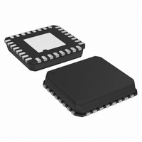
AD9237BCPZRL7-65 Analog Devices Inc, AD9237BCPZRL7-65 Datasheet - Page 18

AD9237BCPZRL7-65
Manufacturer Part Number
AD9237BCPZRL7-65
Description
IC,A/D CONVERTER,SINGLE,12-BIT,CMOS,LLCC,32PIN
Manufacturer
Analog Devices Inc
Datasheet
1.AD9237BCPZRL7-20.pdf
(24 pages)
Specifications of AD9237BCPZRL7-65
Number Of Bits
12
Sampling Rate (per Second)
65M
Data Interface
Parallel
Number Of Converters
3
Power Dissipation (max)
190mW
Voltage Supply Source
Single Supply
Operating Temperature
-40°C ~ 85°C
Mounting Type
Surface Mount
Package / Case
32-VFQFN, CSP Exposed Pad
Lead Free Status / RoHS Status
Lead free / RoHS Compliant
AD9237
Table 7. Reference Configuration Summary
Selected Mode
External Reference
Internal Fixed Reference
Programmable Reference
Internal Fixed Reference
VOLTAGE REFERENCE
A stable and accurate 0.5 V voltage reference is built into
the AD9237. The input range can be adjusted by varying
the reference voltage applied to the AD9237, using either the
internal reference or an externally applied reference voltage.
The input span of the ADC tracks reference voltage changes
linearly.
In all reference configurations, REFT and REFB drive the
A/D conversion core and, in conjunction with the span factor,
establish its input span. The input range of the ADC always
equals four times the voltage at the reference pin divided by
the span factor for either an internal or an external reference.
It is required to decouple REFT to REFB with 0.1 μF and 10 μF
decoupling capacitors, as shown in Figure 39.
Internal Reference Connection
A comparator within the AD9237 detects the potential at
the SENSE pin and configures the reference into one of four
possible states, which are summarized in Table 7. If SENSE is
grounded, the reference amplifier switch is connected to the
internal resistor divider, setting VREF to 1 V (see Figure 39).
Connecting the SENSE pin to VREF switches the reference
amplifier output to the SENSE pin, completing the loop and
providing a 0.5 V reference output. If a resistor divider is
connected, as shown in Figure 40, then the switch is again set to
the SENSE pin. This puts the reference amplifier in a non-
inverting mode with the VREF output defined as
VREF
=
0
.
5
×
⎛ +
⎜
⎝
1
R
R
2
1
⎞
⎟
⎠
SENSE Voltage
AVDD
VREF
0.2 V to VREF
AGND to 0.2 V
Resulting VREF (V)
N/A
0.5
0.5 × (1 + R2/R1)
(See Figure 40)
1.0
Rev. A | Page 18 of 24
10μF
10μF
Span Factor
2
1
2
1
2
1
2
1
+
+
SENSE
Figure 40. Programmable Reference Configuration
0.1μF
SENSE
0.1μF
VREF
VIN+
VIN–
VREF
R2
R1
Figure 39. Internal Reference Configuration
VIN+
VIN–
Resulting Differential Span (V p-p)
1.0 V
4.0 V
2.0 V
1.0 V
Span
4 ×
SELECT
LOGIC
SELECT
4 ×
LOGIC
External
Span
VREF
_
Factor
AD9237
AD9237
_
Factor
Reference
CORE
ADC
CORE
ADC
0.5V
0.5V
REFT
REFB
REFT
REFB
0.1μF
0.1μF
0.1μF
0.1μF
0.1μF
0.1μF
+
+
10μF
10μF


