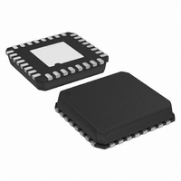
AD9237BCPZRL7-65 Analog Devices Inc, AD9237BCPZRL7-65 Datasheet - Page 8

AD9237BCPZRL7-65
Manufacturer Part Number
AD9237BCPZRL7-65
Description
IC,A/D CONVERTER,SINGLE,12-BIT,CMOS,LLCC,32PIN
Manufacturer
Analog Devices Inc
Datasheet
1.AD9237BCPZRL7-20.pdf
(24 pages)
Specifications of AD9237BCPZRL7-65
Number Of Bits
12
Sampling Rate (per Second)
65M
Data Interface
Parallel
Number Of Converters
3
Power Dissipation (max)
190mW
Voltage Supply Source
Single Supply
Operating Temperature
-40°C ~ 85°C
Mounting Type
Surface Mount
Package / Case
32-VFQFN, CSP Exposed Pad
Lead Free Status / RoHS Status
Lead free / RoHS Compliant
AD9237
PIN CONFIGURATION AND FUNCTION DESCRIPTIONS
Table 6. Pin Function Descriptions
Pin Number
1
2
3
4
5
6
7 to 14, 17 to 20
15
16
21
22
23
24
25
26
27, 32
28, 31
29
30
EP
OTR
Mnemonic
MODE2
CLK
OE
PDWN
GC
DNC
D0 (LSB) to D11 (MSB)
DGND
DRVDD
MODE
SENSE
VREF
REFB
REFT
AVDD
AGND
VIN+
VIN−
Description
SHA Gain Select and Power Scaling Control (see Table 8).
Clock Input Pin.
Output Enable Pin (Active Low).
Power-Down Function Selection (see Table 9).
Gray Code Control (Active High).
Do Not Connect.
Digital Output Ground.
Digital Output Driver Supply. Must be decoupled to DGND with a minimum 0.1 μF capacitor.
Recommended decoupling is 0.1 μF in parallel with 10 μF.
Out-of-Range Indicator.
Data Format and Clock Duty Cycle Stabilizer (DCS) Mode Selection (see Table 10).
Reference Mode Selection (see Table 7).
Voltage Reference Input/Output (see Table 7).
Differential Reference (−). Must be decoupled to REFT with a minimum 10 μF capacitor.
Differential Reference (+).
Analog Power Supply. Must be decoupled to AGND with a minimum 0.1 μF capacitor.
Recommended decoupling is 0.1 μF in parallel with 10 μF.
Analog Ground.
Analog Input Pin (+).
Analog Input Pin (−).
It is recommended that the exposed paddle be soldered to the ground plane. There is an
increased reliability of the solder joints and maximum thermal capability of the package is
achieved with exposed paddle soldered to the customer board.
Data Output Bits.
D0 (LSB)
NOTES
1. DNC = DO NOT CONNECT.
2. IT IS RECOMMENDED THAT THE EXPOSED PADDLE
MODE2
PDWN
BE SOLDERED TO THE GROUND PLANE.
DNC
CLK
OE
GC
D1
1
2
3
4
5
6
7
8
Figure 3. Pin Configuration
Rev. A | Page 8 of 24
(Not to Scale)
PIN 1
INDICATOR
AD9237
TOP VIEW
24 VREF
23 SENSE
22 MODE
21 OTR
20 D11 (MSB)
19 D10
18 D9
17 D8


