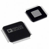
AD9726BSVZRL Analog Devices Inc, AD9726BSVZRL Datasheet - Page 10

AD9726BSVZRL
Manufacturer Part Number
AD9726BSVZRL
Description
IC,D/A CONVERTER,SINGLE,16-BIT,CMOS,TQFP,80PIN
Manufacturer
Analog Devices Inc
Series
TxDAC+®r
Datasheet
1.AD9726BSVZRL.pdf
(24 pages)
Specifications of AD9726BSVZRL
Number Of Bits
16
Data Interface
Parallel
Number Of Converters
1
Voltage Supply Source
Analog and Digital
Power Dissipation (max)
575mW
Operating Temperature
-40°C ~ 85°C
Mounting Type
Surface Mount
Package / Case
80-TQFP Exposed Pad, 80-eTQFP, 80-HTQFP, 80-VQFP
Lead Free Status / RoHS Status
Lead free / RoHS Compliant
For Use With
AD9726-EBZ - BOARD EVAL FOR AD9726
Settling Time
-
Lead Free Status / RoHS Status
Lead free / RoHS Compliant
Available stocks
Company
Part Number
Manufacturer
Quantity
Price
Company:
Part Number:
AD9726BSVZRL
Manufacturer:
Analog Devices Inc
Quantity:
10 000
AD9726
Pin
No.
43
44
45
46
47
48
49
50
51
52
53
54
55
56
57
58
59
60
61
62
63
64
65
66
67
68
Mnemonic
DB4−
DB3+
DB3−
DB2+
DB2−
DB1+
DB1−
DB0+
DB0−
DVDD
DGND
SDO (SYNCALRM)
SDIO
SCLK (SYNCUPD)
CSB
RESET
REFIO
FSADJ
SDR_EN
ADVDD
ADGND
ACVDD
ACGND
AVDD2
AGND2
AVDD1
Description
Data Bit 4 Complement
Data Bit 3 True
Data Bit 3 Complement
Data Bit 2 True
Data Bit 2 Complement
Data Bit 1 True
Data Bit 1 Complement
Data Bit 0 True
Data Bit 0 Complement
Digital Supply Voltage
Digital Supply Common
SPI Data Output (SYNCALRM)
SPI Data Input/Output
SPI Clock Input (SYNCUPD)
SPI Chip Select Bar (Active Low)
Hardware Reset (Active High)
Internal Reference Input/Output
Output Current Full-Scale Adjust
Single Data Rate Mode Enable
Analog Supply Voltage
Analog Supply Common
Analog Supply Voltage
Analog Supply Common
Analog Supply Voltage
Analog Supply Common
Analog Supply Voltage
3
4
2
7
Rev. B | Page 10 of 24
5
6
Pin
No.
69
70
71
72
73
74
75
76
77
78
79
80
1
2
3
4
5
6
7
8
Nominally 1 kΩ to DBGND (may be omitted if data clock output is unused).
SDO is output in 4-wire SPI mode and three-state in 3-wire SPI mode. If SPI is
disabled (SPI_DIS = ADVDD), the alternate pin function is SYNCALRM output.
SDIO is input only in 4-wire SPI mode and bidirectional in 3-wire SPI mode.
If SPI is disabled (SPI_DIS = ADVDD), the alternate pin function is SYNCUPD.
Bypass with 0.1 μF to AGND1. Use the buffer amp to drive external circuitry.
Limit the output current to 1 μA. Apply an external reference to this pin.
Nominally 2 kΩ to AGND1 for 20 mA full-scale output (internal reference).
If SPI is disabled, tie the pin to ADVDD to enable SDR. Otherwise, tie to
ADGND.
Tie the pin to ADVDD to disable SPI; otherwise, tie to ADGND.
Mnemonic
AGND1
IOUTB
IOUTA
AGND1
AVDD1
AGND2
AVDD2
ACGND
ACVDD
ADGND
ADVDD
SPI_DIS
EPAD
Serial Port Interface Disable
Description
Analog Supply Common
Analog Current Output Complement
Analog Current Output True
Analog Supply Common
Analog Supply Voltage
Analog Supply Common
Analog Supply Voltage
Analog Supply Common
Analog Supply Voltage
Analog Supply Common
Analog Supply Voltage
Analog Ground. Serves as an
electrical connection to the
substrate of the die and should be
connected to ground for electrical
and thermal purposes.
8


