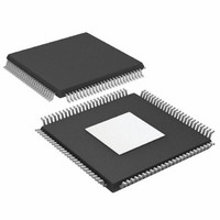
AD9778ABSVZ Analog Devices Inc, AD9778ABSVZ Datasheet - Page 46

AD9778ABSVZ
Manufacturer Part Number
AD9778ABSVZ
Description
IC,D/A CONVERTER,DUAL,14-BIT,CMOS,TQFP,100PIN
Manufacturer
Analog Devices Inc
Specifications of AD9778ABSVZ
Number Of Bits
14
Data Interface
Parallel
Number Of Converters
2
Voltage Supply Source
Analog and Digital
Power Dissipation (max)
300mW
Operating Temperature
-40°C ~ 85°C
Mounting Type
Surface Mount
Package / Case
100-TQFP Exposed Pad, 100-eTQFP, 100-HTQFP, 100-VQFP
Package
100TQFP EP
Resolution
14 Bit
Conversion Rate
1 GSPS
Architecture
Interpolation Filter
Digital Interface Type
Parallel
Number Of Outputs Per Chip
2
Output Type
Current
Full Scale Error
±2(Typ) %FSR
Integral Nonlinearity Error
±1.5(Typ) LSB
Lead Free Status / RoHS Status
Lead free / RoHS Compliant
For Use With
AD9778A-EBZ - BOARD EVALUATION AD9778A
Settling Time
-
Lead Free Status / RoHS Status
Lead free / RoHS Compliant
Available stocks
Company
Part Number
Manufacturer
Quantity
Price
Company:
Part Number:
AD9778ABSVZ
Manufacturer:
Analog Devices Inc
Quantity:
135
Company:
Part Number:
AD9778ABSVZ
Manufacturer:
Analog Devices Inc
Quantity:
10 000
Part Number:
AD9778ABSVZ
Manufacturer:
ADI/亚德诺
Quantity:
20 000
Company:
Part Number:
AD9778ABSVZRL
Manufacturer:
Analog Devices Inc
Quantity:
10 000
AD9776A/AD9778A/AD9779A
SYNCHRONIZING DEVICES TO A SYSTEM CLOCK
The AD9776A/AD9778A/AD9779A offer a pulse mode synchro-
nization scheme (see Figure 89) to align the DAC outputs of
multiple devices within a system to the same DAC clock edge.
The internal clocks are synchronized by providing either a one
time pulse or periodic signal to the SYNC_I inputs (SYNC_I+,
SYNC_I−). The SYNC_I signal is sampled by the internal
DACCLK sample rate clock.
The SYNC_I input frequency has the following constraint:
When the internal clocks are synchronized, the data sampling
clocks between all devices are phase aligned. The data input
timing relationships can be referenced to either REFCLK or
DATACLK.
For this synchronization scheme, all devices are slave devices,
while the system clock generation/distribution chip serves as
the master. It is vital that the SYNC_I signal be distributed
between the DACs with low skew. Likewise, the REFCLK
signals must be distributed with low skew. Any skew on these
signals between the DACs must be accounted for in the timing
budget. Figure 89 shows an example clock and synchronization
input scheme.
f
SYNC
_
I
≤
f
DATA
Figure 90. Timing Diagram of SYNC_I with Respect to REFCLK Synchronizing Multiple Devices to Each Other
GENERATOR
SYSTEM CLOCK
PULSE
DACCLK
REFCLK
SYNC_I
Figure 89. Multichip Synchronization in Pulse Mode
CLOCK DRIVER
CLOCK DRIVER
LOW SKEW
LOW SKEW
Rev. A | Page 46 of 60
t
S_SYNC
MATCHED
LENGTH TRACES
MATCHED
LENGTH TRACES
Figure 90 shows the timing of the SYNC_I input with respect to
the REFCLK input. Note that although the timing is relative to
the REFCLK signal, SYNC_I is sampled at the DACCLK rate.
This means that the rising edge of the SYNC_I signal must occur
after the hold time of the preceding DACCLK rising edge and
not the preceding REFCLK rising edge.
INTERRUPT REQUEST OPERATION
The IRQ pin (Pin 71) acts as an alert in the event that the
device has a timing error and should be queried (by reading
Register 0x19) to determine the exact fault condition. The IRQ
pin is an open-drain, active low output. The IRQ pin should be
pulled high external to the device. This pin can be tied to the
IRQ pins of other devices with open-drain outputs to wire-OR
these pins together.
There are two different error flags that can trigger an interrupt
request, a data timing error or a sync timing error. By default,
when either or both of these error flags are set, the IRQ pin is
active low. Either or both of these error flags can be masked to
prevent them from activating an interrupt on the IRQ pin.
The error flags are latched and remain active until the Interrupt
register, Register 0x19, is either read from or the error flag bits
are overwritten.
t
H_SYNC
REFCLK
SYNC_I
REFCLK
SYNC_I
OUT
OUT


