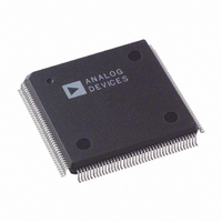
AD9887AKSZ-140 Analog Devices Inc, AD9887AKSZ-140 Datasheet - Page 20

AD9887AKSZ-140
Manufacturer Part Number
AD9887AKSZ-140
Description
IC,TV/VIDEO CIRCUIT,Video Digitizer,CMOS,QFP,160PIN,PLASTIC
Manufacturer
Analog Devices Inc
Datasheet
1.AD9887AKSZ-140.pdf
(52 pages)
Specifications of AD9887AKSZ-140
Applications
Graphic Cards, VGA Interfaces
Interface
Analog and Digital
Voltage - Supply
3.15 V ~ 3.45 V
Package / Case
160-MQFP, 160-PQFP
Mounting Type
Surface Mount
Lead Free Status / RoHS Status
Lead free / RoHS Compliant
Available stocks
Company
Part Number
Manufacturer
Quantity
Price
Company:
Part Number:
AD9887AKSZ-140
Manufacturer:
MAX
Quantity:
59
Company:
Part Number:
AD9887AKSZ-140
Manufacturer:
ADI
Quantity:
364
Company:
Part Number:
AD9887AKSZ-140
Manufacturer:
Analog Devices Inc
Quantity:
10 000
Part Number:
AD9887AKSZ-140
Manufacturer:
ADI/亚德诺
Quantity:
20 000
AD9887A
Any jitter in the clock reduces the precision with which the
sampling time can be determined and, thus, must be subtracted
from the stable pixel time. The AD9887A clock generation
circuit is designed to minimize jitter to less than 6% of the total
pixel time in all operating modes, making its effect on valid
sampling time negligible (see Figure 10).
The PLL characteristics are determined by the loop-filter design,
the PLL charge-pump current, and the VCO range setting. The
loop-filter design is illustrated in Figure 11. Recommended settings
of VCO range and charge-pump current for VESA standard
display modes are listed in Table 7.
The following programmable registers are provided to optimize
the performance of the PLL:
•
The 12-Bit Divisor Register. The input Hsync frequencies
range from 15 kHz to 110 kHz. The PLL multiplies the
frequency of the Hsync signal, producing pixel clock
frequencies in the range of 12 MHz to 170 MHz. The
divisor register controls the exact multiplication factor. This
register can be set to any value between 221 and 4095. (The
divide ratio used is the programmed divide ratio plus one.)
6
5
4
3
2
1
0
0.0039μF
Figure 10. Pixel Clock Jitter vs. Frequency
C
Figure 11. PLL Loop-Filter Detail
P
PIXEL CLOCK (MHz)
0.039μF
FILT
C
Z
R
3.3kΩ
Z
PV
D
Rev. B | Page 20 of 52
•
Table 5. VCO Frequency Ranges
PV1
0
0
1
1
•
Table 6. Charge-Pump Current/Control Bits
Ip2
0
0
0
0
1
1
1
1
•
The 2-Bit VCO Range Register. To lower the sensitivity of
the output frequency to noise on the control signal, the VCO
operating frequency range is divided into four overlapping
regions. The VCO range register sets this operating range.
Because there are only three possible regions, just 2 LSBs of
the VCO range register are used. The frequency ranges for
the lowest and highest regions are shown in Table 5.
The 3-Bit Charge-Pump Current Register. This register
allows the current that drives the low-pass loop filter to be
varied. The possible current values are listed in Table 6.
The 5-Bit Phase Adjust Register. The phase of the
generated sampling clock can be shifted to locate an
optimum sampling point within a clock cycle. The phase-
adjust register provides 32 phase-shift steps of 11.25° each.
The Hsync signal with an identical phase shift is available
through the HSOUT pin. Phase adjustment is operational
even if the pixel clock is provided externally. The COAST
signal allows the PLL to continue to run at the same frequency
in the absence of the incoming Hsync signal. This can be
used during the vertical sync period or any other time that
the Hsync signal is unavailable. The polarity of the coast
signal can be set through the COAST polarity bit, and the
polarity of the Hsync signal can be set through the HSYNC
polarity bit. If not using automatic polarity detection, set
the HSYNC and COAST polarity bits to match the polarity
of their respective signals.
Ip1
0
0
1
1
0
0
1
1
PV0
0
1
0
1
Ip0
0
1
0
1
0
1
0
1
Pixel Clock Range (MHz)
12 to 37
37 to 74
74 to 140
140 to 170
Current (μA)
50
100
150
250
350
500
750
1500


