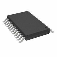
ADF7011BRU-REEL Analog Devices Inc, ADF7011BRU-REEL Datasheet - Page 17

ADF7011BRU-REEL
Manufacturer Part Number
ADF7011BRU-REEL
Description
IC,RF Modulator,CMOS,TSSOP,24PIN,PLASTIC
Manufacturer
Analog Devices Inc
Datasheet
1.ADF7011BRUZ-RL.pdf
(24 pages)
Specifications of ADF7011BRU-REEL
Rohs Status
RoHS non-compliant
Frequency
433 ~ 435MHz; 866 ~ 870MHz
Applications
Data Transfer, RKE, Remote Control/Security Systems
Modulation Or Protocol
ASK, FSK, GFSK, OOK
Data Rate - Maximum
76.8 kbps
Power - Output
-16dBm ~ 12dBm
Current - Transmitting
34mA
Data Interface
PCB, Surface Mount
Antenna Connector
PCB, Surface Mount
Voltage - Supply
2.3 V ~ 3.6 V
Operating Temperature
-40°C ~ 85°C
Package / Case
24-TSSOP
Features
-
Memory Size
-
Lead Free Status / RoHS Status
Voltage Controlled Oscillator (VCO)
An on-chip VCO is included on the transmitter. The VCO con-
verts the control voltage generated by the loop filter into an output
frequency that is sent to the antenna via the power amplifier
(PA). The VCO has a typical gain of 80 MHz/V and operates
from 866 MHz to 870 MHz. The PD1 bit in the function regis-
ter is the active high bit that turns on the VCO. A frequency
divided by 2 is included to allow operation in the lower 450 MHz
band. To enable operation in the lower band, the V1 bit in the
N Register should be set to 1.
The VCO needs an external 220 nF between the VCO and the
regulator to reduce internal noise.
RF Output Stage
The RF output stage consists of a DAC with a number of cur-
rent sources to adjust the output power level. To set up the
power level
The output stage is powered down by setting Bit PD2 in the
function register to zero.
REV. 0
VCO CONTROL BIT
LOOP FILTER
• FSK GFSK: The output power is set using the modulation
• ASK: The output power as set up for FSK is the output
Register by entering a 7-bit number into Bits P1–P7. The
two MSBs set the range of the output stage, while the five
LSBs set the output power in the selected range.
power for a TxDATA of 1. The output power for a zero
data bit is set up the same way but using Bits D1–D7.
C
REG
220nF
Figure 7. Voltage Controlled Oscillator
PIN
VCO
DIVIDE
BY 2
VCO SELECT BIT
MUX
TO PA AND
N DIVIDER
–17–
Serial Interface
The serial interface allows the user to program the four 24-bit
registers using a 3-wire interface (CLK, Data, and Load Enable).
The serial interface consists of a level shifter, a 24-bit shift regis-
ter, and four latches. Signals should be CMOS compatible. The
serial interface is powered by the regulator, and therefore is
inactive when CE is low.
Data is clocked into the shift register, MSB first, on the rising
edge of each clock (CLK). Data is transferred to one of four
latches on the rising edge of LE. The destination latch is deter-
mined by the value of the two control bits (C2 and C1). These
are the two LSBs, DB1 and DB0, as shown in the timing dia-
gram of Figure 1.
P5
C2
0
0
1
1
Figure 9. Output Stage Matching
PA
Table I. C2, C1 Truth Table
Figure 8. Output Stage
C1
0
1
0
1
V
P1
DD
RF
OUT
Data Latch
R Register
N Register
Modulation Register
Function Register
L1
L2
HIGH
LOW
MED
C1
P7, P6
ADF7011
50


