ADG1236YCPZ-500RL7 Analog Devices Inc, ADG1236YCPZ-500RL7 Datasheet - Page 7
ADG1236YCPZ-500RL7
Manufacturer Part Number
ADG1236YCPZ-500RL7
Description
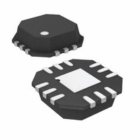
IC,ANALOG SWITCH,DUAL,SPDT,CMOS,LLCC,12PIN,PLASTIC
Manufacturer
Analog Devices Inc
Series
iCMOS®r
Type
Analog Switchr
Datasheet
1.ADG1236YCPZ-500RL7.pdf
(16 pages)
Specifications of ADG1236YCPZ-500RL7
Function
Switch
Circuit
2 x SPDT
On-state Resistance
260 Ohm
Voltage Supply Source
Single Supply
Voltage - Supply, Single/dual (±)
12V, 15V
Current - Supply
1µA
Operating Temperature
-40°C ~ 125°C
Mounting Type
Surface Mount
Package / Case
12-VFQFN, CSP Exposed Pad
Multiplexer Configuration
Dual SPDT
Number Of Inputs
2
Number Of Outputs
4
Number Of Channels
2
Analog Switch On Resistance
475@10.8VOhm
Analog Switch Turn On Time
150ns
Analog Switch Turn Off Time
190ns
Package Type
LFCSP
Power Supply Requirement
Single/Dual
Single Supply Voltage (typ)
12V
Dual Supply Voltage (typ)
±15V
Power Dissipation
3.5mW
Supply Current
0.23mA
Mounting
Surface Mount
Pin Count
12
Operating Temp Range
-40C to 125C
Operating Temperature Classification
Automotive
Lead Free Status / RoHS Status
Lead free / RoHS Compliant
Lead Free Status / RoHS Status
Lead free / RoHS Compliant
Other names
ADG1236YCPZ-500RL7TR


PIN CONFIGURATIONS AND FUNCTION DESCRIPTIONS
Table 5. Pin Function Descriptions
TSSOP
1
2
3
4
5
6
7, 8, 14 to 16
9
10
11
12
13
Pin No.
LFCSP
11
12
1
2
3
4
10
5
6
7
8
9
Figure 2. TSSOP Pin Configuration
GND
S1A
S1B
V
IN1
NC
NC
D1
SS
NC = NO CONNECT
1
2
3
4
5
6
7
8
(Not to Scale)
ADG1236
TOP VIEW
Mnemonic
IN1
S1A
D1
S1B
V
GND
NC
IN2
S2A
D2
S2B
V
SS
DD
16
15
14
13
12
11
10
9
NC
NC
NC
V
S2B
D2
S2A
IN2
DD
Description
Logic Control Input.
Source Terminal. Can be an input or output.
Drain Terminal. Can be an input or output.
Source Terminal. Can be an input or output.
Most Negative Power Supply Potential.
Ground (0 V) Reference.
No Connect.
Logic Control Input.
Source Terminal. Can be an input or output.
Drain Terminal. Can be an input or output.
Source Terminal. Can be an input or output.
Most Positive Power Supply Potential.
Rev. 0 | Page 7 of 16
NOTES
1. EXPOSED PAD TIED TO SUBSTRATE, V
NC = NO CONNECT
Figure 3. LFCSP Pin Configuration
S1B
V
D1
SS
1
2
3
(Not to Scale)
ADG1236
TOP VIEW
PIN 1
INDICATOR
9 V
8 S2B
7 D2
SS
DD
.
ADG1236
Related parts for ADG1236YCPZ-500RL7
Image
Part Number
Description
Manufacturer
Datasheet
Request
R

Part Number:
Description:
IC,ANALOG SWITCH,DUAL,SPDT,CMOS,LLCC,12PIN,PLASTIC
Manufacturer:
Analog Devices Inc
Datasheet:

Part Number:
Description:
±1.7g Dual-Axis IMEMS Accelerometer Evaluation Board
Manufacturer:
Analog Devices Inc
Datasheet:

Part Number:
Description:
Inertial Sensor Evaluation System
Manufacturer:
Analog Devices Inc
Datasheet:
Part Number:
Description:
Manufacturer:
Analog Devices Inc
Datasheet:
Part Number:
Description:
Manufacturer:
Analog Devices Inc
Datasheet:
Part Number:
Description:
Manufacturer:
Analog Devices Inc
Datasheet:
Part Number:
Description:
Manufacturer:
Analog Devices Inc
Datasheet:
Part Number:
Description:
Manufacturer:
Analog Devices Inc
Datasheet:
Part Number:
Description:
Manufacturer:
Analog Devices Inc
Datasheet:
Part Number:
Description:
Manufacturer:
Analog Devices Inc
Datasheet:
Part Number:
Description:
Manufacturer:
Analog Devices Inc
Datasheet:
Part Number:
Description:
Manufacturer:
Analog Devices Inc
Datasheet:
Part Number:
Description:
Manufacturer:
Analog Devices Inc
Datasheet: