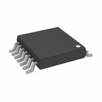
ADG1404YRUZ Analog Devices Inc, ADG1404YRUZ Datasheet - Page 4

ADG1404YRUZ
Manufacturer Part Number
ADG1404YRUZ
Description
+/-15V 4:1 Mux With Ron Max = 2 Ohm
Manufacturer
Analog Devices Inc
Series
iCMOS®r
Datasheet
1.ADG1404YRUZ.pdf
(16 pages)
Specifications of ADG1404YRUZ
Function
Multiplexer
Circuit
1 x 4:1
On-state Resistance
1.8 Ohm
Voltage Supply Source
Single Supply
Voltage - Supply, Single/dual (±)
12V, 15V
Current - Supply
1µA
Operating Temperature
-40°C ~ 125°C
Mounting Type
Surface Mount
Package / Case
14-TSSOP (0.173", 4.40mm Width)
Lead Free Status / RoHS Status
Lead free / RoHS Compliant
Available stocks
Company
Part Number
Manufacturer
Quantity
Price
Part Number:
ADG1404YRUZ
Manufacturer:
ADI/亚德诺
Quantity:
20 000
ADG1404
12 V SINGLE SUPPLY
V
Table 2.
Parameter
ANALOG SWITCH
LEAKAGE CURRENTS
DYNAMIC CHARACTERISTICS
POWER REQUIREMENTS
1
Guaranteed by design, not subject to production test.
DD
Analog Signal Range
On Resistance (R
On-Resistance Match
On-Resistance Flatness (R
Source Off Leakage, I
Drain Off Leakage, I
Channel On Leakage, I
DIGITAL INPUTS
Input High Voltage, V
Input Low Voltage, V
Input Current, I
Digital Input Capacitance, C
Transition Time, t
t
t
Break-Before-Make Time Delay, t
Charge Injection
Off Isolation
Channel-to-Channel Crosstalk
−3 dB Bandwidth
Insertion Loss
C
C
C
I
I
V
DD
DD
ON
OFF
DD
S
D
D
= 12 V ± 10%, V
, C
Between Channels (ΔR
(Off)
(Off)
(EN)
(EN)
S
(On)
INL
ON
TRANSITION
or I
)
D
SS
INL
INH
S
(Off)
INH
= 0 V, GND = 0 V, unless otherwise noted.
(Off)
D
, I
S
ON
FLAT(ON)
(On)
1
)
IN
BBM
)
25°C
2.8
3.5
0.13
0.21
0.6
1.1
±0.02
±0.55
±0.03
±0.55
±0.1
±1.5
0.001
3.5
230
300
180
240
115
160
100
30
80
82
35
−0.3
39
150
217
0.001
170
−40°C to +85°C
4.3
0.23
1.2
±2
±4
±4
375
295
190
Rev. A | Page 4 of 16
−40°C to +125°C
0 V to V
4.8
0.25
1.3
±12.5
±30
±30
2.0
0.8
±0.1
430
335
220
10
1
285
5/16.5
DD
Unit
V
Ω typ
Ω max
Ω typ
Ω max
Ω typ
Ω max
nA typ
nA max
nA typ
nA max
nA typ
nA max
V min
V max
μA typ
μA max
pF typ
ns typ
ns max
ns typ
ns max
ns typ
ns max
ns typ
ns min
pC typ
dB typ
dB typ
MHz typ
dB typ
pF typ
pF typ
pF typ
μA typ
μA max
μA typ
μA max
V min/max
Test Conditions/Comments
V
V
V
V
V
V
V
V
V
R
V
R
V
R
V
R
V
V
R
R
R
R
f = 1 MHz, V
f = 1 MHz, V
f = 1 MHz, V
V
Digital inputs = 0 V or V
Digital inputs = 5 V
GND = 0 V, V
L
L
L
S
DD
S
S
DD
S
S
S
IN
L
S
L
S
L
S
L
S1
S
L
DD
= 50 Ω, C
= 50 Ω, C
= 1 V/10 V, V
= 1 V/10 V, V
= 50 Ω, C
= V
= 300 Ω, C
= 8 V; see
= 300 Ω, C
= 8 V; see
= 300 Ω, C
= 8 V; see
= 300 Ω, C
= 6 V, R
= 50 Ω, C
= 0 V to 10 V, I
= 0 V to 10 V, I
= 0V to 10 V, I
= V
= V
= 10.8 V, V
= 13.2 V, V
= 13.2 V
D
GND
S2
= 1 V or 10 V; see
= 8 V; see
or V
S
L
L
L
= 0 Ω, C
L
= 5 pF, f = 100 kHz; see
= 5 pF, f = 1 MHz; see
S
S
S
= 5 pF, f = 100 kHz; see
Figure 29
Figure 31
Figure 31
SS
L
L
L
L
= 5 pF; see
= 6 V
= 6 V
= 6 V
DD
= 35 pF
= 35 pF
= 35 pF
= 35 pF
SS
SS
D
D
= 0 V
= 10 V/1 V; see
= 10 V/1 V; see
S
= 0 V
= 0 V
S
= −10 mA; see
S
= −10 mA
= −10 mA
Figure 30
L
= 1 nF; see
DD
Figure 26
Figure 24
Figure 23
Figure 23
Figure 22
Figure 32
Figure 26
Figure 27
Figure 25


