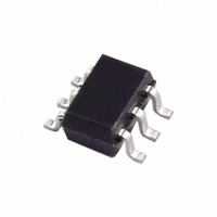
ADG849YKSZ-REEL7 Analog Devices Inc, ADG849YKSZ-REEL7 Datasheet - Page 5

ADG849YKSZ-REEL7
Manufacturer Part Number
ADG849YKSZ-REEL7
Description
IC,ANALOG SWITCH,SINGLE,SPDT,CMOS,TSSOP,6PIN,PLASTIC
Manufacturer
Analog Devices Inc
Type
Analog Switchr
Datasheet
1.ADG849YKSZ-REEL.pdf
(12 pages)
Specifications of ADG849YKSZ-REEL7
Function
Switch
Circuit
1 x SPDT
On-state Resistance
600 mOhm
Voltage Supply Source
Single Supply
Voltage - Supply, Single/dual (±)
5V
Current - Supply
0.001µA
Operating Temperature
-40°C ~ 125°C
Mounting Type
Surface Mount
Package / Case
6-TSSOP, SC-88, SOT-363
Multiplexer Configuration
Single SPDT
Number Of Inputs
1
Number Of Outputs
2
Number Of Channels
1
Analog Switch On Resistance
1.1@3.6VOhm
Analog Switch Turn On Time
22ns
Analog Switch Turn Off Time
18ns
Package Type
SC-70
Power Supply Requirement
Single
Single Supply Voltage (min)
1.8V
Single Supply Voltage (typ)
3/5V
Single Supply Voltage (max)
5.5V
Dual Supply Voltage (min)
Not RequiredV
Dual Supply Voltage (typ)
Not RequiredV
Dual Supply Voltage (max)
Not RequiredV
Power Dissipation
0.00001W
Supply Current
0.001mA
Mounting
Surface Mount
Pin Count
6
Operating Temp Range
-40C to 125C
Operating Temperature Classification
Automotive
Package
6SC-70
Maximum On Resistance
1.1@3.6V Ohm
Maximum High Level Output Current
400 mA
Maximum Turn-off Time
18@3.6V ns
Maximum Turn-on Time
22@3.6V ns
Switch Architecture
SPDT
Power Supply Type
Single
Lead Free Status / RoHS Status
Lead free / RoHS Compliant
Lead Free Status / RoHS Status
Lead free / RoHS Compliant
Available stocks
Company
Part Number
Manufacturer
Quantity
Price
Company:
Part Number:
ADG849YKSZ-REEL7
Manufacturer:
ON
Quantity:
400
Part Number:
ADG849YKSZ-REEL7
Manufacturer:
ADI/亚德诺
Quantity:
20 000
ABSOLUTE MAXIMUM RATINGS
Table 3. T
Parameter
V
Analog Inputs
Digital Inputs
Peak Current, S or D
Continuous Current, S or D
Operating Temperature Range
SC70 Package
Reflow Soldering
1
ESD CAUTION
ESD (electrostatic discharge) sensitive device. Electrostatic charges as high as 4000 V readily accumulate on
the human body and test equipment and can discharge without detection. Although this product features
proprietary ESD protection circuitry, permanent damage may occur on devices subjected to high energy
electrostatic discharges. Therefore, proper ESD precautions are recommended to avoid performance
degradation or loss of functionality.
Overvoltages at IN, S, or D will be clamped by internal diodes. Current
should be limited to the maximum ratings given.
DD
Extended
Storage Temperature Range
Junction Temperature
θ
θ
Peak Temperature
Time at Peak Temperature
to GND
JA
JC
Thermal Impedance
Thermal Impedance
A
= 25°C, unless otherwise noted
1
1
Rating
–0.3 V to +7 V
–0.3 V to V
whichever occurs first
–0.3 V to V
whichever occurs first
600 mA (pulsed at 1 ms,
10% duty cycle maximum)
400 mA
–40°C to +125°C
–65°C to +150°C
+150°C
332°C/W
120°C/W
260(0/–5)°C
10 sec to 40 sec
DD
DD
+ 0.3 V or 30 mA,
+ 0.3 V or 30 mA,
Rev. 0| Page 5 of 12
Table 4. Truth Table
IN
0
1
Stresses above those listed under Absolute Maximum Ratings
may cause permanent damage to the device. This is a stress
rating only; functional operation of the device at these or any
other conditions above those listed in the operational sections
of this specification is not implied. Exposure to absolute
maximum rating conditions for extended periods may affect
device reliability. Only one absolute maximum rating may be
applied at any one time.
Switch S1
On
Off
Switch S2
Off
On
ADG849


