ADG849YKSZ-500RL7 Analog Devices Inc, ADG849YKSZ-500RL7 Datasheet
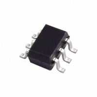
IC SWITCH SPDT SC70-6

ADG849YKSZ-500RL7

Manufacturer Part Number
ADG849YKSZ-500RL7
Description
IC SWITCH SPDT SC70-6
Manufacturer
Analog Devices Inc
Type
Analog Switchr
Datasheet

Specifications of ADG849YKSZ-500RL7

Function
Switch
Circuit
1 x SPDT
On-state Resistance
600 mOhm
Voltage Supply Source
Single Supply
Voltage - Supply, Single/dual (±)
5V
Current - Supply
0.001µA
Operating Temperature
-40°C ~ 125°C
Mounting Type
Surface Mount
Package / Case
6-TSSOP, SC-88, SOT-363
Analog Switch Type
SPDT
No. Of Channels
1
Bandwidth
38MHz
On State Resistance Max
0.5ohm
Turn Off Time
9ns
Turn On Time
11ns
Supply Voltage Range
1.8V To 5.5V
Multiplexer Configuration
Single SPDT
Number Of Inputs
1
Number Of Outputs
2
Number Of Channels
1
Analog Switch On Resistance
1.1@3.6VOhm
Analog Switch Turn On Time
22ns
Analog Switch Turn Off Time
18ns
Package Type
SC-70
Power Supply Requirement
Single
Single Supply Voltage (min)
1.8V
Single Supply Voltage (typ)
3/5V
Single Supply Voltage (max)
5.5V
Dual Supply Voltage (min)
Not RequiredV
Dual Supply Voltage (typ)
Not RequiredV
Dual Supply Voltage (max)
Not RequiredV
Power Dissipation
0.00001W
Supply Current
0.001mA
Mounting
Surface Mount
Pin Count
6
Operating Temp Range
-40C to 125C
Operating Temperature Classification
Automotive
Lead Free Status / RoHS Status
Lead free / RoHS Compliant
Lead Free Status / RoHS Status
Lead free / RoHS Compliant, Lead free / RoHS Compliant
Other names
ADG849YKSZ500RLTR

Available stocks

Company
Part Number
Manufacturer
Quantity
Price
Part Number:
ADG849YKSZ-500RL7
Manufacturer:
Maxim
Quantity:
149
FEATURES
Ultralow on-resistance:
Excellent audio performance, ultralow distortion:
High current carrying capability:
Automotive temperature range: –40°C to +125°C
Rail-to-rail operation
Typical power consumption (<0.01 µW)
Pin-compatible upgrade for the ADG749 and ADG779
APPLICATIONS
Cellular phones
PDAs
Battery-powered systems
Audio and video signal routing
Modems
PCMCIA cards
Hard drives
Relay replacement
GENERAL DESCRIPTION
The ADG849 is a monolithic, CMOS SPDT (single pole, double
throw) switch that operates with a supply range of 1.8 V to 5.5 V.
It is designed to offer ultralow on-resistance values of typically
0.5 Ω. This design makes the ADG849 an ideal solution for
applications that require minimal distortion through the switch.
The ADG849 also has the capability of carrying large amounts
of current, typically 600 mA at 5 V operation.
Each switch of the ADG849 conducts equally well in both
directions when on. The device exhibits break-before-make
switching action, thus preventing momentary shorting when
switching channels.
The ADG849 is available in a tiny, 6-lead SC70 package, making
it the ideal candidate for space-constrained applications.
Rev. 0
Information furnished by Analog Devices is believed to be accurate and reliable.
However, no responsibility is assumed by Analog Devices for its use, nor for any
infringements of patents or other rights of third parties that may result from its use.
Specifications subject to change without notice. No license is granted by implication
or otherwise under any patent or patent rights of Analog Devices. Trademarks and
registered trademarks are the property of their respective owners.
0.5 Ω typical
0.8 Ω maximum at 5 V supply
0.13 Ω typical
0.24 Ω maximum R
400 mA continuous current
600 mA peak current at 5 V
ON
flatness
PRODUCT HIGHLIGHTS
1.
2.
3.
4.
5.
One Technology Way, P.O. Box 9106, Norwood, MA 02062-9106, U.S.A.
Tel: 781.329.4700
Fax: 781.326.8703
Very low on-resistance, 0.5 Ω typical.
Tiny, 6-lead SC70 package.
Low power dissipation. The CMOS construction ensures
low power dissipation.
High current carrying capability.
Low THD + noise (0.01% typ).
0.5 Ω SPDT/2:1 Mux in SC70
FUNCTIONAL BLOCK DIAGRAM
© 2004 Analog Devices, Inc. All rights reserved.
S2
S1
IN
SWITCHES SHOWN
FOR A LOGIC 1 INPUT
ADG849
Figure 1.
3 V/5 V CMOS
D
www.analog.com
ADG849

Related parts for ADG849YKSZ-500RL7

ADG849YKSZ-500RL7 Summary of contents

Page 1

FEATURES Ultralow on-resistance: 0.5 Ω typical 0.8 Ω maximum supply Excellent audio performance, ultralow distortion: 0.13 Ω typical 0.24 Ω maximum R flatness ON High current carrying capability: 400 mA continuous current 600 mA peak current at ...

Page 2

ADG849 TABLE OF CONTENTS Specifications..................................................................................... 3 Absolute Maximum Ratings............................................................ 5 ESD Caution.................................................................................. 5 Pin Configuration and Function Descriptions............................. 6 REVISION HISTORY 7/04—Revision 0: Initial Version Typical Performance Characteristics ..............................................7 Test Circuits........................................................................................9 Outline Dimensions ....................................................................... 11 Ordering Guide .......................................................................... 11 Rev. ...

Page 3

SPECIFICATIONS Table 4 5.5 V, GND = Parameter ANALOG SWITCH Analog Signal Range On-Resistance ( On-Resistance Match Between Channels (∆ On-Resistance Flatness (R ) FLAT(ON) LEAKAGE CURRENTS Source ...

Page 4

ADG849 Table 2 3.6 V, GND = Parameter ANALOG SWITCH Analog Signal Range On-Resistance ( On-Resistance Match Between Channels (∆ On-Resistance Flatness (R ) FLAT(ON) LEAKAGE CURRENTS Source ...

Page 5

ABSOLUTE MAXIMUM RATINGS Table 25°C, unless otherwise noted A Parameter Rating V to GND –0 Analog Inputs –0 whichever occurs first Digital Inputs –0 ...

Page 6

ADG849 PIN CONFIGURATION AND FUNCTION DESCRIPTIONS Table 5. Terminology Mnemonic Function V Most Positive Power Supply Potential. DD GND Ground (0 V) Reference. I Positive Supply Current Source Terminal. May be an input or output. D Drain Terminal. ...

Page 7

TYPICAL PERFORMANCE CHARACTERISTICS 0 25°C A 0.5 4.5V 5V 0.4 5.5V 0.3 0 Figure 3. On-Resistance vs 0.9 0.8 2.5V 0.7 ...

Page 8

ADG849 250 T = 25°C A 200 150 100 0.5 1.0 1.5 2.0 2.5 3.0 DRAIN VOLTAGE (V) Figure 9. Charge Injection OFF ...

Page 9

TEST CIRCUITS V1 Figure 15. On-Resistance V 0.1µ GND V DD 0.1µ GND ...

Page 10

ADG849 V DD 0.1µ 50Ω GND V OUT OFF ISOLATION = 20 LOG VS Figure 21. Off Isolation NETWORK ANALYZER NETWORK ANALYZER V OUT 50Ω OUT R L 50Ω CHANNEL-TO-CHANNEL CROSSTALK ...

Page 11

... OUTLINE DIMENSIONS 0.10 MAX ORDERING GUIDE Model Temperature Range 2 ADG849YKSZ-500RL7 –40°C to +125°C 2 ADG849YKSZ-REEL –40°C to +125°C 2 ADG849YKSZ-REEL7 –40°C to +125°C 1 Branding on all packages is limited to three characters due to space constraints Pb-free part. 2.00 BSC 2.10 BSC 1.25 BSC ...

Page 12

ADG849 NOTES © 2004 Analog Devices, Inc. All rights reserved. Trademarks and registered trademarks are the property of their respective owners. D04737-0-7/04(0) Rev. 0| Page ...

Related keywords