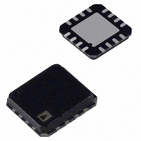
ADL5561ACPZ-R7 Analog Devices Inc, ADL5561ACPZ-R7 Datasheet - Page 7

ADL5561ACPZ-R7
Manufacturer Part Number
ADL5561ACPZ-R7
Description
Low Distortion 3V 41mA Diff Amp
Manufacturer
Analog Devices Inc
Datasheet
1.ADL5561ACPZ-R7.pdf
(24 pages)
Specifications of ADL5561ACPZ-R7
Amplifier Type
RF/IF Differential
Number Of Circuits
1
Output Type
Differential
Slew Rate
9800 V/µs
-3db Bandwidth
2.9GHz
Current - Input Bias
3µA
Current - Supply
40mA
Voltage - Supply, Single/dual (±)
3 V ~ 3.6 V
Operating Temperature
-40°C ~ 85°C
Mounting Type
Surface Mount
Package / Case
16-VFQFN, 16-CSP, Exposed Pad
Voltage - Supply
3 V ~ 3.6 V
Frequency
2.9GHz
Rf Type
General Purpose
Gain
15.5dB
Noise Figure
8dB
P1db
19dBm
Lead Free Status / RoHS Status
Lead free / RoHS Compliant
Test Frequency
-
Lead Free Status / RoHS Status
Lead free / RoHS Compliant
Other names
ADL5561ACPZ-R7TR
Available stocks
Company
Part Number
Manufacturer
Quantity
Price
Company:
Part Number:
ADL5561ACPZ-R7
Manufacturer:
MICREL
Quantity:
1 000
Part Number:
ADL5561ACPZ-R7
Manufacturer:
ADI/亚德诺
Quantity:
20 000
PIN CONFIGURATION AND FUNCTION DESCRIPTIONS
Table 3. Pin Function Descriptions
Pin No.
1
2
3
4
5, 6, 7, 8
9
10
11
12
13, 14, 15, 16
Mnemonic
VIP2
VIP1
VIN1
VIN2
VCC
VCOM
VON
VOP
ENBL
GND
EP
Description
Balanced Differential Input. Biased to VCOM, typically ac-coupled. Input for A
VIP1 for A
Balanced Differential Input. Biased to VCOM, typically ac-coupled. Input for A
VIP2 for A
Balanced Differential Input. Biased to VCOM, typically ac-coupled. Input for A
VIN2 for A
Balanced Differential Input. Biased to VCOM, typically ac-coupled. Input for A
VIN1 for A
Positive Supply.
Common-Mode Voltage. A voltage applied to this pin sets the common-mode voltage of the input and
output. Typically decoupled to ground with a 0.1 μF capacitor. With no reference applied, input and
output common mode floats to midsupply (VCC/2).
Balanced Differential Output. Biased to VCOM, typically ac-coupled.
Balanced Differential Output. Biased to VCOM, typically ac-coupled.
Enable. Apply positive voltage (1.0 V < ENBL < VCC) to activate device.
Ground. Connect to low impedance ground.
Exposed Paddle. Connect to a low impedance thermal and electrical ground plane.
v
v
v
v
= 15.5 dB.
= 15.5 dB.
= 15.5 dB.
= 15.5 dB.
NOTES
1. EXPOSED PADDLE. CONNECT TO A LOW
VIP2
VIP1
VIN1
VIN2
IMPEDANCE THERMAL AND ELECTRICAL
GROUND PLANE.
1
2
3
4
Figure 2. Pin Configuration
Rev. B | Page 7 of 24
(Not to Scale)
ADL5561
TOP VIEW
PIN 1
INDICATOR
12 ENBL
11 VOP
10 VON
9 VCOM
V
V
V
V
= 12 dB gain, strapped to
= 6 dB gain, strapped to
= 6 dB gain, strapped to
= 12 dB gain, strapped to
ADL5561


