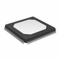
ADSP-21060LKSZ-160 Analog Devices Inc, ADSP-21060LKSZ-160 Datasheet - Page 18

ADSP-21060LKSZ-160
Manufacturer Part Number
ADSP-21060LKSZ-160
Description
IC,DSP,32-BIT,CMOS,QFP,240PIN,PLASTIC
Manufacturer
Analog Devices Inc
Series
SHARC®r
Type
Floating Pointr
Specifications of ADSP-21060LKSZ-160
Interface
Host Interface, Link Port, Serial Port
Clock Rate
40MHz
Non-volatile Memory
External
On-chip Ram
512kB
Voltage - I/o
3.30V
Voltage - Core
3.30V
Operating Temperature
0°C ~ 85°C
Mounting Type
Surface Mount
Package / Case
240-MQFP, 240-PQFP
Device Core Size
32b
Architecture
Super Harvard
Format
Floating Point
Clock Freq (max)
40MHz
Mips
40
Device Input Clock Speed
40MHz
Ram Size
512KB
Program Memory Size
Not RequiredKB
Operating Supply Voltage (typ)
3.3V
Operating Supply Voltage (min)
3.15V
Operating Supply Voltage (max)
3.45V
Operating Temp Range
0C to 85C
Operating Temperature Classification
Commercial
Mounting
Surface Mount
Pin Count
240
Package Type
MQFP
Lead Free Status / RoHS Status
Lead free / RoHS Compliant
Lead Free Status / RoHS Status
Lead free / RoHS Compliant
Available stocks
Company
Part Number
Manufacturer
Quantity
Price
Company:
Part Number:
ADSP-21060LKSZ-160
Manufacturer:
Analog Devices Inc
Quantity:
10 000
ADSP-21060/ADSP-21060L/ADSP-21062/ADSP-21062L/ADSP-21060C/ADSP-21060LC
ADSP-21060L/ADSP-21062L SPECIFICATIONS
Note that component specifications are subject to change
without notice.
OPERATING CONDITIONS (3.3 V)
1
2
ELECTRICAL CHARACTERISTICS (3.3 V)
1
2
3
4
5
6
7
8
9
10
11
12
Applies to input and bidirectional pins: DATA47–0, ADDR31–0, RD, WR, SW, ACK, SBTS, IRQ2–0, FLAG3–0, HGB, CS, DMAR1, DMAR2, BR6–1, ID2–0, RPBA, CPA,
Applies to input pins: CLKIN, RESET, TRST
Applies to output and bidirectional pins: DATA47–0, ADDR31–0, MS3–0, RD, WR, PAGE, ADRCLK, SW, ACK, FLAG3–0, TIMEXP, HBG, REDY, DMAG1, DMAG2,
See “Output Drive Currents” for typical drive current capabilities.
Applies to input pins: ACK, SBTS, IRQ2–0, HBR, CS, DMAR1, DMAR2, ID2–0, RPBA, EBOOT, LBOOT, CLKIN, RESET, TCK.
Applies to input pins with internal pull-ups: DR0, DR1, TRST, TMS, TDI.
Applies to three-statable pins: DATA47–0, ADDR31–0, MS3–0, RD, WR, PAGE, ADRCLK, SW, ACK, FLAG3–0, HBG, REDY, DMAG1, DMAG2, BMS, BR6–1, TFSx, RFSx,
Applies to three-statable pins with internal pull-ups: DT0, DT1, TCLK0, TCLK1, RCLK0, RCLK1.
Applies to CPA pin.
Applies to ACK pin when pulled up. (Note that ACK is pulled up internally with 2 k: during reset in a multiprocessor system, when ID2–0 = 001 and another ADSP-2106xL
Applies to three-statable pins with internal pull-downs: LxDAT3–0, LxCLK, LxACK.
Applies to ACK pin when keeper latch enabled.
Applies to all signal pins.
Guaranteed but not tested.
Parameter
V
T
V
V
V
Parameter
V
V
I
I
I
I
I
I
I
I
I
I
C
TFS0, TFS1, RFS0, RFS1, LxDAT3–0, LxCLK, LxACK, EBOOT, LBOOT, BMS, TMS, TDI, TCK, HBR, DR0, DR1, TCLK0, TCLK1, RCLK0, RCLK1
BR6–1, CPA, DT0, DT1, TCLK0, TCLK1, RCLK0, RCLK1, TFS0, TFS1, RFS0, RFS1, LxDAT3–0, LxCLK, LxACK, BMS, TDO, EMU, ICSA.
TDO, EMU. (Note that ACK is pulled up internally with 2 k: during reset in a multiprocessor system, when ID2–0 = 001 and another ADSP-2106x is not requesting bus
mastership.)
is not requesting bus mastership).
IH
IL
ILP
OZH
OZL
OZHP
OZLC
OZLA
OZLAR
OZLS
CASE
DD
IH
IH
IL
OH
OL
IN
3
3, 4
4
1
2
11, 12
1, 2
5, 9
1, 2
1, 2
5, 6, 7, 8
6
7
10
1
2
9
8
Description
Supply Voltage
Case Operating Temperature
High Level Input Voltage @ V
High Level Input Voltage @ V
Low Level Input Voltage @ V
Description
High Level Output Voltage
Low Level Output Voltage
High Level Input Current
Low Level Input Current
Low Level Input Current
Three-State Leakage Current
Three-State Leakage Current
Three-State Leakage Current
Three-State Leakage Current
Three-State Leakage Current
Three-State Leakage Current
Three-State Leakage Current
Input Capacitance
DD
DD
DD
= Min
= Max
= Max
Rev. F | Page 18 of 64 | March 2008
Min
3.15
–40
2.0
2.2
–0.5
Test Conditions
@ V
@ V
@ V
@ V
@ V
@ V
@ V
@ V
@ V
@ V
@ V
@ V
f
IN
= 1 MHz, T
A Grade
Max
3.45
+85
V
V
+0.8
DD
DD
DD
DD
DD
DD
DD
DD
DD
DD
DD
DD
DD
DD
= Min, I
= Min, I
= Max, V
= Max, V
= Max, V
= Max, V
= Max, V
= Max, V
= Max, V
= Max, V
= Max, V
= Max, V
+ 0.5
+ 0.5
CASE
OH
OL
IN
IN
IN
IN
IN
IN
IN
IN
IN
IN
= 4.0 mA
= –2.0 mA
= V
= 0 V
= 0 V
= V
= 0 V
= V
= 0 V
= 1.5 V
= 0 V
= 0 V
= 25°C, V
DD
DD
DD
–40
Min
3.15
2.0
2.2
–0.5
Max
Max
Max
IN
= 2.5 V
C Grade
Max
3.45
+100
V
V
+0.8
DD
DD
+ 0.5
+ 0.5
Min
3.15
–40
2.0
2.2
–0.5
Min
2.4
K Grade
Max
3.45
+85
V
V
+0.8
DD
DD
+ 0.5
+ 0.5
Max
0.4
10
10
150
10
10
350
1.5
350
4.2
150
4.7
Unit
V
V
μA
μA
μA
μA
μA
μA
mA
μA
mA
μA
pF
Unit
V
qC
V
V
V


