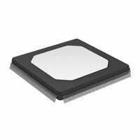
ADSP-21061KSZ-133 Analog Devices Inc, ADSP-21061KSZ-133 Datasheet - Page 35

ADSP-21061KSZ-133
Manufacturer Part Number
ADSP-21061KSZ-133
Description
ADSP-21061 1MBIT, 33MHz, 5v SHARC
Manufacturer
Analog Devices Inc
Series
SHARC®r
Type
Floating Pointr
Datasheet
1.ADSP-21061LKSZ-160.pdf
(56 pages)
Specifications of ADSP-21061KSZ-133
Interface
Synchronous Serial Port (SSP)
Clock Rate
33MHz
Non-volatile Memory
External
On-chip Ram
128kB
Voltage - I/o
5.00V
Voltage - Core
5.00V
Operating Temperature
0°C ~ 85°C
Mounting Type
Surface Mount
Package / Case
240-MQFP, 240-PQFP
Package
240MQFP
Numeric And Arithmetic Format
Floating-Point
Maximum Speed
33 MHz
Ram Size
128 KB
Device Million Instructions Per Second
33 MIPS
Lead Free Status / RoHS Status
Lead free / RoHS Compliant
Available stocks
Company
Part Number
Manufacturer
Quantity
Price
Company:
Part Number:
ADSP-21061KSZ-133
Manufacturer:
Analog Devices Inc
Quantity:
10 000
Three-State Timing—Bus Master, Bus Slave, HBR, SBTS
These specifications show how the memory interface is disabled
(stops driving) or enabled (resumes driving) relative to CLKIN
and the SBTS pin. This timing is applicable to bus master transi-
tion cycles (BTC) and host transition cycles (HTC) as well as the
SBTS pin.
Table 19. Three-State Timing—Bus Master, Bus Slave
1
2
3
Parameter
Timing Requirements
t
t
Switching Characteristics
t
t
t
t
t
t
t
t
t
t
t
t
t
t
Strobes = RD, WR, PAGE, DMAGx, MSx, BMS, SW.
In addition to bus master transition cycles, these specs also apply to bus master and bus slave synchronous read/write.
Memory Interface = Address, RD, WR, MSx, SW, PAGE, DMAGx, and BMS (in EPROM boot mode).
STSCK
HTSCK
MIENA
MIENS
MIENHG
MITRA
MITRS
MITRHG
DATEN
DATTR
ACKEN
ACKTR
ADCEN
ADCTR
MTRHBG
MENHBG
SBTS Setup Before CLKIN
SBTS Hold Before CLKIN
Address/Select Enable After CLKIN
Strobes Enable After CLKIN
HBG Enable After CLKIN
Address/Select Disable After CLKIN
Strobes Disable After CLKIN
HBG Disable After CLKIN
Data Enable After CLKIN
Data Disable After CLKIN
ACK Enable After CLKIN
ACK Disable After CLKIN
ADRCLK Enable After CLKIN
ADRCLK Disable After CLKIN
Memory Interface Disable Before HBG Low
Memory Interface Enable After HBG High
INTERFACE
MEMORY
CLKOUT
CLKIN
DATA
SBTS
ACK
Figure 21. Three-State Timing (Bus Transition Cycle, SBTS Assertion)
2
2
2
2
1
1
t
ADCEN
t
t
ACKEN
MIENA,
t
DATEN
Rev. C | Page 35 of 56 | July 2007
t
MIENS,
3
t
3
MIENHG
t
STSCK
t
HTSCK
t
Min
12 + DT/2
–1 – DT/8
–1.5 – DT/8
–1.5 – DT/8
9 + 5DT/16
0 – DT/8
7.5 + DT/4
–1 – DT/8
–2 – DT/8
0 + DT/8
19 + DT
t
DATTR
ACKTR
t
ADSP-21061/ADSP-21061L
t
ADCTR
MITRA,
t
MITRS,
5 V and 3.3 V
t
MITRHG
Max
6 + DT/2
0 – DT/4
1.5 – DT/4
2.0 – DT/4
7 – DT/8
6 – DT/8
8 – DT/4
Unit
ns
ns
ns
ns
ns
ns
ns
ns
ns
ns
ns
ns
ns
ns
ns
ns


