ADSP-21261SKBCZ150 Analog Devices Inc, ADSP-21261SKBCZ150 Datasheet - Page 3
ADSP-21261SKBCZ150
Manufacturer Part Number
ADSP-21261SKBCZ150
Description
150 MHz, 32Bit DSP Processor
Manufacturer
Analog Devices Inc
Series
SHARC®r
Type
Fixed/Floating Pointr
Specifications of ADSP-21261SKBCZ150
Interface
DAI, SPI
Clock Rate
150MHz
Non-volatile Memory
ROM (384 kB)
On-chip Ram
128kB
Voltage - I/o
3.30V
Voltage - Core
1.20V
Operating Temperature
0°C ~ 70°C
Mounting Type
Surface Mount
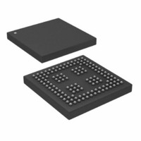
Package / Case
136-CSPBGA
Device Core Size
32/40Bit
Architecture
Super Harvard
Format
Floating Point
Clock Freq (max)
150MHz
Mips
150
Device Input Clock Speed
150MHz
Ram Size
128KB
Program Memory Size
384KB
Operating Supply Voltage (typ)
1.2/3.3V
Operating Supply Voltage (min)
1.14/3.13V
Operating Supply Voltage (max)
1.26/3.47V
Operating Temp Range
0C to 70C
Operating Temperature Classification
Commercial
Mounting
Surface Mount
Pin Count
136
Package Type
CSPBGA
Lead Free Status / RoHS Status
Lead free / RoHS Compliant
Lead Free Status / RoHS Status
Lead free / RoHS Compliant
Available stocks
Company
Part Number
Manufacturer
Quantity
Price
Company:

Part Number:
ADSP-21261SKBCZ150
Manufacturer:
Analog Devices Inc
Quantity:
10 000
Part Number:
ADSP-21261SKBCZ150
Manufacturer:
ADI/亚德诺
Quantity:
20 000


TABLE OF CONTENTS
General Description ................................................. 4
Pin Function Descriptions ........................................ 11
ADSP-21261 Specifications ....................................... 15
ADSP-21261 Family Core Architecture ...................... 4
ADSP-21261 Memory and I/O Interface Features ......... 6
Target Board JTAG Emulator Connector .................... 8
Development Tools ............................................... 8
Evaluation Kit ..................................................... 10
Designing an Emulator-Compatible
Additional Information ......................................... 10
Address Data Pins as Flags ..................................... 14
Boot Modes ........................................................ 14
Core Instruction Rate to CLKIN Ratio Modes ............. 14
Address Data Modes ............................................. 14
Recommended Operating Conditions ....................... 15
Electrical Characteristics ........................................ 15
Absolute Maximum Ratings ................................... 16
ESD Sensitivity .................................................... 16
Timing Specifications ........................................... 17
SIMD Computational Engine ............................... 4
Independent, Parallel Computation Units ................ 4
Data Register File ............................................... 5
Single-Cycle Fetch of Instruction and
Instruction Cache .............................................. 5
Data Address Generators with Zero-Overhead
Flexible Instruction Set ....................................... 6
Dual-Ported On-Chip Memory ............................. 6
DMA Controller ................................................ 6
Digital Applications Interface (DAI) ....................... 6
Serial Ports ....................................................... 6
Serial Peripheral (Compatible) Interface .................. 7
Parallel Port ..................................................... 7
Timers ............................................................ 8
Program Booting ............................................... 8
Phase-Locked Loop ............................................ 8
Power Supplies .................................................. 8
DSP Board (Target) ........................................... 10
Power-Up Sequencing ....................................... 18
Clock Input ..................................................... 19
Clock Signals ................................................... 19
Four Operands ............................................... 5
Hardware Circular Buffer Support ...................... 5
Rev. 0 | Page 3 of 44 | March 2006
136-Ball BGA Pin Configurations ............................... 39
144-Lead LQFP Pin Configurations ............................ 42
Package Dimensions ............................................... 43
Ordering Guide ..................................................... 44
REVISION HISTORY
3/06—Rev. 0: Initial Release
Output Drive Currents ......................................... 37
Test Conditions .................................................. 37
Capacitive Loading .............................................. 37
Environmental Conditions .................................... 38
Thermal Characteristics ........................................ 38
Surface Mount Design .......................................... 44
Reset ............................................................. 20
Interrupts ....................................................... 20
Core Timer ..................................................... 20
Timer PWM_OUT Cycle Timing ......................... 21
Timer WDTH_CAP Timing ............................... 21
DAI Pin-to-Pin Direct Routing ............................ 22
Precision Clock Generator (Direct Pin Routing) ...... 23
Flags ............................................................. 24
Memory Read—Parallel Port ............................... 25
Memory Write—Parallel Port ............................. 27
Serial Ports ..................................................... 29
Input Data Port (IDP) ....................................... 32
Parallel Data Acquisition Port (PDAP) .................. 33
SPI Protocol—Master ........................................ 34
SPI Protocol—Slave .......................................... 34
JTAG Test Access Port and Emulation .................. 36
ADSP-21261
Related parts for ADSP-21261SKBCZ150
Image
Part Number
Description
Manufacturer
Datasheet
Request
R

Part Number:
Description:
±1.7g Dual-Axis IMEMS Accelerometer Evaluation Board
Manufacturer:
Analog Devices Inc
Datasheet:

Part Number:
Description:
Inertial Sensor Evaluation System
Manufacturer:
Analog Devices Inc
Datasheet:
Part Number:
Description:
Manufacturer:
Analog Devices Inc
Datasheet:
Part Number:
Description:
Manufacturer:
Analog Devices Inc
Datasheet:
Part Number:
Description:
Manufacturer:
Analog Devices Inc
Datasheet:
Part Number:
Description:
Manufacturer:
Analog Devices Inc
Datasheet:
Part Number:
Description:
Manufacturer:
Analog Devices Inc
Datasheet:
Part Number:
Description:
Manufacturer:
Analog Devices Inc
Datasheet:
Part Number:
Description:
Manufacturer:
Analog Devices Inc
Datasheet:
Part Number:
Description:
Manufacturer:
Analog Devices Inc
Datasheet:
Part Number:
Description:
Manufacturer:
Analog Devices Inc
Datasheet:
Part Number:
Description:
Manufacturer:
Analog Devices Inc
Datasheet:
Part Number:
Description:
Manufacturer:
Analog Devices Inc
Datasheet: