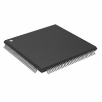
ADSP-2191MBSTZ-140 Analog Devices Inc, ADSP-2191MBSTZ-140 Datasheet - Page 41

ADSP-2191MBSTZ-140
Manufacturer Part Number
ADSP-2191MBSTZ-140
Description
IC,DSP,16-BIT,CMOS,QFP,144PIN,PLASTIC
Manufacturer
Analog Devices Inc
Series
ADSP-21xxr
Type
Fixed Pointr
Specifications of ADSP-2191MBSTZ-140
Interface
Host Interface, SPI, SSP, UART
Clock Rate
140MHz
Non-volatile Memory
External
On-chip Ram
160kB
Voltage - I/o
3.00V, 3.30V
Voltage - Core
2.50V
Operating Temperature
-40°C ~ 85°C
Mounting Type
Surface Mount
Package / Case
144-LQFP
Device Core Size
16b
Clock Freq (max)
140MHz
Mips
140
Device Input Clock Speed
140MHz
Ram Size
160KB
Operating Supply Voltage (typ)
2.5/3.3V
Operating Supply Voltage (min)
2.37/2.97V
Operating Supply Voltage (max)
2.63/3.6V
Operating Temp Range
-40C to 85C
Operating Temperature Classification
Industrial
Mounting
Surface Mount
Pin Count
144
Package Type
LQFP
Lead Free Status / RoHS Status
Lead free / RoHS Compliant
Lead Free Status / RoHS Status
Lead free / RoHS Compliant
Other names
ADSP-2191MBSTZ140
Available stocks
Company
Part Number
Manufacturer
Quantity
Price
Company:
Part Number:
ADSP-2191MBSTZ-140
Manufacturer:
MAXIM
Quantity:
101
Company:
Part Number:
ADSP-2191MBSTZ-140
Manufacturer:
Analog Devices Inc
Quantity:
10 000
Output Drive Currents
Figure 25
of the ADSP-2191M. The curves represent the current drive
capability of the output drivers as a function of output voltage.
Figure 25. Typical Drive Currents
Power Dissipation
Total power dissipation has two components, one due to internal
circuitry and one due to the switching of external output drivers.
Internal power dissipation is dependent on the instruction
execution sequence and the data operands involved.
Table 23. P
A typical power consumption can now be calculated for these
conditions by adding a typical internal power dissipation with the
following formula.
Where:
Note that the conditions causing a worst-case P
from those causing a worst-case P
occur while 100% of the output pins are switching from all ones
to all zeros. Note also that it is not common for an application to
have 100% or even 50% of the outputs switching simultaneously.
REV. 0
Pin Type
Address
MSx
WR
Data
CLKOUT
P
P
listed in
EXT
INT
–100
–20
–40
–60
–80
60
40
20
is I
is from
0
shows typical I-V characteristics for the output drivers
0
Power Dissipation on page
DDINT
EXT
0.5
# of Pins
15
1
1
16
1
Table 23
Calculation Example
P
OUTPUT CURRENT
TOTAL
1.0
SOURCE (
2.5 V, using the calculation I
INPUT CURRENT
1.5
=
V
V
VDDEXT
DDEXT
P
OL
EXT
% Switching
50
0
—
50
—
2.0
INT
) VOLTAGE – V
= 3.65V @
+
V
V
V
V
. Maximum P
DDEXT
DDEXT
DDEXT
DDEXT
2.5
P
V
DDEXT
INT
41.
– 40°C
= 3.0V @
= 3.0V @
= 3.3V @
= 3.65V @
3.0
= 3.3V @
V
EXT
OH
3.5
+ 85°C
+ 85°C
+ 25°C
– 40°C
are different
+ 25°C
INT
DDINT
10 pF
10 pF
10 pF
10 pF
10 pF
4.0
cannot
C
–41–
The external component of total power dissipation is caused by
the switching of output pins. Its magnitude depends on:
and is calculated by the formula below.
The load capacitance includes the processor’s package capaci-
tance (C
high and then back low. Address and data pins can drive high and
low at a maximum rate of 1/(2t
every cycle at a frequency of 1/t
but selects can switch on each cycle. For example, estimate P
with the following assumptions:
The P
drive as shown in
Test Conditions
The DSP is tested for output enable, disable, and hold time.
Output Disable Time
Output pins are considered to be disabled when they stop driving,
go into a high impedance state, and start to decay from their
output high or low voltage. The time for the voltage on the bus
to decay by – V is dependent on the capacitive load, C
load current, I
equation below.
The maximum frequency at which they can switch (f)
Their load capacitance (C)
Their voltage swing (V
A system with one bank of external data memory—asyn-
chronous RAM (16-bit)
One 64K 16 RAM chip is used with a load of 10 pF
Maximum peripheral speed CCLK = 80 MHz, HCLK =
80 MHz
External data memory writes occur every other cycle, a
rate of 1/(4t
The bus cycle time is 80 MHz (t
Number of output pins that switch during each cycle (O)
20 MHz
20 MHz
40 MHz
20 MHz
80 MHz
EXT
f
IN
). The switching frequency includes driving the load
equation is calculated for each class of pins that can
L
HCLK
. This decay time can be approximated by the
Table
P
EXT
), with 50% of the pins switching
t
DECAY
23.
=
10.9 V
10.9 V
10.9 V
10.9 V
10.9 V
DD
V
O C
DD
CK
)
CK
=
2
. Select pins switch at 1/(2t
). The write strobe can switch
C
---------------
ADSP-2191M
V
L
I
L
HCLK
DD
V
= P
= .01635 W
= 0 W
= .00436 W
= .01744 W
= .00872 W
P
2
EXT
f
= 12.5 nsec)
EXT
=.04687 W
L
and the
CK
EXT
),


