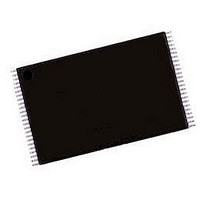
AM29LV065DU90REF Spansion Inc., AM29LV065DU90REF Datasheet - Page 22

AM29LV065DU90REF
Manufacturer Part Number
AM29LV065DU90REF
Description
Flash Memory IC
Manufacturer
Spansion Inc.
Datasheet
1.AM29LV065DU90REF.pdf
(54 pages)
Specifications of AM29LV065DU90REF
Memory Size
64Mbit
Memory Configuration
8M X 8
Ic Interface Type
Parallel
Access Time
90ns
Memory Case Style
TSOP
No. Of Pins
48
Operating Temperature Range
-40°C To +85°C
Termination Type
SMD
Lead Free Status / RoHS Status
Lead free / RoHS Compliant
Available stocks
Company
Part Number
Manufacturer
Quantity
Price
Company:
Part Number:
AM29LV065DU90REF
Manufacturer:
INFINEON
Quantity:
201
Part Number:
AM29LV065DU90REF
Manufacturer:
SPANSIO
Quantity:
20 000
Hardware Data Protection
The command sequence requirement of unlock cycles
for programming or erasing provides data protection
against inadvertent writes (refer to
COMMON FLASH MEMORY INTERFACE (CFI)
The Common Flash Interface (CFI) specification out-
lines device and host system software interrogation
handshake, which allows specific vendor-specified
software algorithms to be used for entire families of
devices. Software support can then be device-inde-
pendent, JEDEC ID-independent, and forward- and
backward-compatible for the specified flash device
families. Flash vendors can standardize their existing
interfaces for long-term compatibility.
This device enters the CFI Query mode when the sys-
tem writes the CFI Query command, 98h, any time the
device is ready to read array data (addresses are don’t
care). The system can read CFI information at the ad-
22
Figure 3. SecSi Sector Protect Verify
Write 40h to SecSi
Read from SecSi
Sector address
Sector address
A1 = 1, A0 = 0
A1 = 1, A0 = 0
Write 60h to
with A6 = 0,
any address
with A6 = 0,
RESET# =
V
Wait 1 μs
START
IH
or V
ID
Remove V
SecSi Sector is
SecSi Sector is
If data = 00h,
If data = 01h,
from RESET#
Protect Verify
SecSi Sector
unprotected.
Write reset
protected.
command
complete
Table 10
IH
or V
ID
for com-
Am29LV065D
mand definitions). In addition, the following hardware
data protection measures prevent accidental erasure
or programming, which might otherwise be caused by
spurious system level signals during V
and power-down transitions, or from system noise.
Low V
When V
cept any write cycles. This protects data during V
power-up and power-down. The command register
and all internal program/erase circuits are disabled,
and the device resets to the read mode. Subsequent
writes are ignored until V
system must provide the proper signals to the control
pins to prevent unintentional writes when V
greater than V
Write Pulse “Glitch” Protection
Noise pulses of less than 5 ns (typical) on OE#, CE#
or WE# do not initiate a write cycle.
Logical Inhibit
Write cycles are inhibited by holding any one of OE# =
V
CE# and WE# must be a logical zero while OE# is a
logical one.
Power-Up Write Inhibit
If WE# = CE# = V
the device does not accept commands on the rising
edge of WE#. The internal state machine is automati-
cally reset to the read mode on power-up.
dresses given in Tables 6–9. To terminate reading CFI
data, the system must write the reset command.
The system can also write the CFI query command
when the device is in the autoselect mode. The device
enters the CFI query mode, and the system can read
CFI data at the addresses given in Tables 6–9. The
system must write the reset command to return the
device to the autoselect mode.
For further information, please refer to the CFI Specifi-
cation and CFI Publication 100, available via the World
Wide Web at http://www.amd.com/flash/cfi.html. Alter-
natively, contact an AMD representative for copies of
these documents.
IL
, CE# = V
CC
CC
Write Inhibit
is less than V
IH
LKO
or WE# = V
.
IL
and OE# = V
LKO
CC
IH
, the device does not ac-
is greater than V
. To initiate a write cycle,
IH
February 16, 2006
during power up,
CC
power-up
LKO
. The
CC
CC
is


