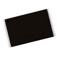
AM29LV641DH120REF Spansion Inc., AM29LV641DH120REF Datasheet - Page 13

AM29LV641DH120REF
Manufacturer Part Number
AM29LV641DH120REF
Description
Flash Memory IC
Manufacturer
Spansion Inc.
Datasheet
1.AM29LV641DH90REI.pdf
(57 pages)
Specifications of AM29LV641DH120REF
Memory Size
64Mbit
Memory Configuration
4M X 16
Ic Interface Type
Parallel
Access Time
120ns
Memory Case Style
TSOP
No. Of Pins
48
Operating Temperature Range
-40°C To +85°C
Termination Type
SMD
Lead Free Status / RoHS Status
Lead free / RoHS Compliant
data on the device data outputs. The device remains
enabled for read access until the command register
contents are altered.
See
page 10
“Read-Only Operations” on page 37
specifications and to
ing diagram. I
page 34
tion for reading array data.
Writing Commands/Command Sequences
To write a command or command sequence (which in-
cludes programming data to the device and erasing
sectors of memory), the system must drive WE# and
CE# to V
The device features an Unlock Bypass mode to facili-
tate faster programming. Once the device enters the
Unlock Bypass mode, only two write cycles are re-
quired to program a word instead of four. The
Program Command Sequence” on page 24
tails on programming data to the device using both
standard and Unlock Bypass command sequences.
An erase operation can erase one sector, multiple sec-
tors, or the entire device.
the address space that each sector occupies.
I
tive current specification for the write mode. The
Characteristics
tables and timing diagrams for write operations.
Accelerated Program Operation
The device offers accelerated program operations
through the ACC function. This function is primarily in-
tended to allow faster manufacturing throughput dur-
ing system production.
If the system asserts V
matically enters the aforementioned Unlock Bypass
mode, temporarily unprotects any protected sectors,
and uses the higher voltage on the pin to reduce the
time required for program operations. The system
would use a two-cycle program command sequence
as required by the Unlock Bypass mode. Removing
V
eration. Note that the ACC pin must not be at V
operations other than accelerated programming, or
device damage may result.
Autoselect Functions
If the system writes the autoselect command se-
quence, the device enters the autoselect mode. The
system can then read autoselect codes from the inter-
nal register (which is separate from the memory array)
on DQ7–DQ0. Standard read cycle timings apply in
this mode. Refer to the
January 22, 2007 22366C6
CC2
HH
from the ACC pin returns the device to normal op-
in the DC Characteristics table represents the ac-
“Requirements for Reading Array Data” on
table represents the active current specifica-
IL
for more infor mation. Refer to the AC
, and OE# to V
CC1
section contains timing specification
in the
Figure 13, on page 37
HH
“Autoselect Mode” on page 16
IH
Table 2 on page 12
on this pin, the device auto-
.
“DC Characteristics” on
table for timing
Am29LV640D/Am29LV641D
for the tim-
D A T A
indicates
has de-
“Word
HH
AC
for
S H E E T
and
more information.
Standby Mode
When the system is not reading or writing to the de-
vice, it can place the device in the standby mode. In
this mode, current consumption is greatly reduced,
and the outputs are placed in the high impedance
state, independent of the OE# input.
The device enters the CMOS standby mode when the
CE# and RESET# pins are both held at V
(Note that this is a more restricted voltage range than
V
V
standby current is greater. The device requires stan-
dard access time (t
vice is in either of these standby modes before it is
ready to read data.
If the device is deselected during erasure or program-
ming, the device draws active current until the
operation is completed.
I
resents the standby current specification.
Automatic Sleep Mode
The automatic sleep mode minimizes Flash device en-
ergy consumption. The device automatically enables
this mode when addresses remain stable for t
30 ns. The automatic sleep mode is independent of
the CE#, WE#, and OE# control signals. Standard ad-
dress access timings provide new data when ad-
dresses are changed. While in sleep mode, output
data is latched and always available to the system.
I
resents the automatic sleep mode current specifica-
tion.
RESET#: Hardware Reset Pin
The RESET# pin provides a hardware method of re-
setting the device to reading array data. When the RE-
SET# pin is driven low for at least a period of t
device immediately terminates any operation in
progress, tristates all output pins, and ignores all
read/write commands for the duration of the RESET#
pulse. The device also resets the internal state ma-
chine to reading array data. To ensure data integrity,
the operation that was interrupted should be reinitiated
once the device is ready to accept another command
sequence.
Current is reduced for the duration of the RESET#
pulse. When RESET# is held at V
draws CMOS standby current (I
at V
greater.
CC3
CC4
IH
CC
.) If CE# and RESET# are held at V
IL
“Autoselect Command Sequence” on page 24
± 0.3 V, the device is in the standby mode, but the
in the table
in the table
but not within V
“DC Characteristics” on page 34
“DC Characteristics” on page 34
CE
SS
) for read access when the de-
±0.3 V, the standby current is
CC4
SS
). If RESET# is held
±0.3 V, the device
IH
, but not within
CC
± 0.3 V.
RP
ACC
, the
rep-
rep-
11
for
+


