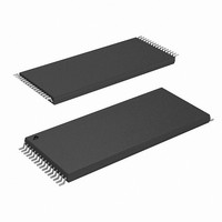
CY62128EV30LL-45ZXIT Cypress Semiconductor Corp, CY62128EV30LL-45ZXIT Datasheet - Page 4

CY62128EV30LL-45ZXIT
Manufacturer Part Number
CY62128EV30LL-45ZXIT
Description
CY62128EV30LL-45ZXIT
Manufacturer
Cypress Semiconductor Corp
Specifications of CY62128EV30LL-45ZXIT
Format - Memory
RAM
Memory Type
SRAM
Memory Size
1M (128K x 8)
Speed
45ns
Interface
Parallel
Voltage - Supply
2.2 V ~ 3.6 V
Operating Temperature
-40°C ~ 85°C
Package / Case
32-TSOP I
Density
1Mb
Access Time (max)
45ns
Sync/async
Asynchronous
Architecture
Not Required
Clock Freq (max)
Not RequiredMHz
Operating Supply Voltage (typ)
3V
Address Bus
17b
Package Type
TSOP-I
Operating Temp Range
-40C to 85C
Number Of Ports
1
Supply Current
16mA
Operating Supply Voltage (min)
2.2V
Operating Supply Voltage (max)
3.6V
Operating Temperature Classification
Industrial
Mounting
Surface Mount
Pin Count
32
Word Size
8b
Number Of Words
128K
Lead Free Status / RoHS Status
Lead free / RoHS Compliant
Lead Free Status / RoHS Status
Lead free / RoHS Compliant
Available stocks
Company
Part Number
Manufacturer
Quantity
Price
Company:
Part Number:
CY62128EV30LL-45ZXIT
Manufacturer:
CRYSTAL
Quantity:
1 408
Part Number:
CY62128EV30LL-45ZXIT
Manufacturer:
CYPRESS/赛普拉斯
Quantity:
20 000
Maximum Ratings
Exceeding maximum ratings may shorten the useful life of the
device. User guidelines are not tested.
Storage temperature ................................ –65 °C to +150 °C
Ambient temperature with
power applied .......................................... –55 °C to +125 °C
Supply voltage to ground
potential .......................................–0.3 V to V
DC voltage applied to outputs
in high Z State
Electrical Characteristics
Over the Operating Range
Notes
Document #: 38-05579 Rev. *J
V
V
V
V
I
I
I
I
I
3. V
4. V
5. Full device AC operation assumes a 100 µs ramp time from 0 to V
6. Typical values are included for reference only and are not guaranteed or tested. Typical values are measured at V
7. Chip enables (CE
IX
OZ
CC
SB1
SB2
Parameter
OH
OL
IH
IL
[7]
[7]
IL(min)
IH(max)
= –2.0 V for pulse durations less than 20 ns.
= V
CC
[3, 4]
+ 0.75 V for pulse durations less than 20 ns.
Output HIGH voltage
Output LOW voltage
Input HIGH voltage
Input LOW voltage
Input leakage current
Output leakage current
V
Automatic CE
power-down
current — CMOS inputs
Automatic CE
power-down
current — CMOS inputs
CC
1
and CE
......................–0.3 V to V
operating supply current
2
) must be at CMOS level to meet the I
Description
CC(max)
CC(max)
I
I
I
I
V
V
V
V
GND < V
GND < V
f = f
f = 1 MHz
CE
V
f = f
f = 0 (OE and WE), V
CE
V
f = 0, V
OH
OH
OL
OL
CC
CC
CC
CC
IN
IN
1
1
+ 0.3 V
+ 0.3 V
= 0.1 mA
= 2.1 mA, V
max
> V
max
= –0.1 mA
= –1.0 mA, V
> V
= 2.7 V to 3.6 V
= 2.7 V to 3.6 V
= 2.2 V to 2.7 V
= 2.2 V to 2.7 V
> V
> V
SB1
CC(min)
CC
CC
CC
= 1/t
(address and data only),
CC
CC
/ I
I
O
< V
SB2
Test Conditions
= 3.60 V
< V
– 0.2 V, V
– 0.2 V or V
0.2 V, CE
and 200 µs wait time after V
– 0.2 V, CE
RC
CC
/ I
CC
CCDR
CC
, output disabled
CC
DC input voltage
Output current into outputs (LOW) ............................. 20 mA
Static discharge voltage
(MIL-STD-883, method 3015) ................................. > 2001 V
Latch-up current .................................................... > 200 mA
Operating Range
> 2.70 V
CY62128EV30LL Industrial –40 °C to +85 °C 2.2 V to 3.6 V
V
I
CMOS levels
spec. Other inputs can be left floating.
OUT
> 2.70 V
CC
IN
CC
< 0.2 V
IN
2
2
= V
= 0 mA
Device
< 0.2 V
= 3.60 V
< 0.2 V
< 0.2 V,
CCmax
CC
stabilization.
[3, 4]
Range
...................–0.3 V to V
–0.3
–0.3
Min
2.0
2.4
1.8
2.2
–1
–1
CC
–
–
–
–
–
–
= V
CY62128EV30 MoBL
45 ns (Industrial)
CC(typ)
Temperature
, T
Typ
Ambient
A
1.3
11
–
–
–
–
–
–
–
–
–
–
1
1
= 25 °C.
[6]
V
V
CC(max)
CC
CC
Max
0.4
0.4
0.6
0.8
2.0
+1
+1
16
+ 0.3 V
+ 0.3 V
–
–
4
4
Page 4 of 18
V
+ 0.3 V
CC
[5]
Unit
mA
mA
µA
µA
µA
µA
V
V
V
V
V
V
V
V
®
[+] Feedback


