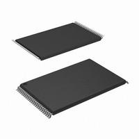
CY62167ELL-45ZXI Cypress Semiconductor Corp, CY62167ELL-45ZXI Datasheet - Page 9

CY62167ELL-45ZXI
Manufacturer Part Number
CY62167ELL-45ZXI
Description
CY62167ELL-45ZXI
Manufacturer
Cypress Semiconductor Corp
Datasheet
1.CY62167ELL-45ZXI.pdf
(15 pages)
Specifications of CY62167ELL-45ZXI
Format - Memory
RAM
Memory Type
SRAM
Memory Size
16M (2M x 8 or 1M x 16)
Speed
45ns
Interface
Parallel
Voltage - Supply
4.5 V ~ 5.5 V
Operating Temperature
-40°C ~ 85°C
Package / Case
48-TSOP I
Density
16Mb
Access Time (max)
45ns
Sync/async
Asynchronous
Architecture
SDR
Clock Freq (max)
Not RequiredMHz
Operating Supply Voltage (typ)
5V
Address Bus
21/20Bit
Package Type
TSOP-I
Operating Temp Range
-40C to 85C
Number Of Ports
1
Supply Current
30mA
Operating Supply Voltage (min)
4.5V
Operating Supply Voltage (max)
5.5V
Operating Temperature Classification
Industrial
Mounting
Surface Mount
Pin Count
48
Word Size
8/16Bit
Number Of Words
2M/1M
Lead Free Status / RoHS Status
Lead free / RoHS Compliant
Lead Free Status / RoHS Status
Lead free / RoHS Compliant
Available stocks
Company
Part Number
Manufacturer
Quantity
Price
Company:
Part Number:
CY62167ELL-45ZXI
Manufacturer:
CYPRESSRESS
Quantity:
5 530
Company:
Part Number:
CY62167ELL-45ZXI
Manufacturer:
CYP
Quantity:
3 586
Company:
Part Number:
CY62167ELL-45ZXI
Manufacturer:
CYPRESS
Quantity:
624
Part Number:
CY62167ELL-45ZXI
Manufacturer:
CYPRESS/赛普拉斯
Quantity:
20 000
Switching Waveforms
Notes
Document Number: 001-15607 Rev. *B
29. The internal write time of the memory is defined by the overlap of WE, CE
30. Data I/O is high impedance if OE = V
31. If CE
32. During this period the I/Os are in output state and input signals must not be applied.
a write and any of these signals can terminate a write by going inactive. The data input setup and hold timing should be referenced to the edge of the signal that
terminates the write.
ADDRESS
ADDRESS
BHE/BLE
BHE/BLE
DATA I/O
DATA I/O
1
goes HIGH and CE
CE
CE
CE
CE
WE
WE
OE
1
2
1
2
NOTE
NOTE
2
32
goes LOW simultaneously with WE = V
32
t
SA
Figure 4. Write Cycle No. 2 (CE
(continued)
IH
Figure 5. Write Cycle No. 3 (WE controlled, OE LOW
.
t
HZOE
t
HZWE
t
SA
t
AW
t
AW
IH
, the output remains in a high impedance state.
t
t
BW
SCE
1
t
= V
t
WC
WC
t
PWE
IL
1
t
, BHE or BLE or both = V
BW
or CE
VALID DATA
t
t
PWE
SD
2
t
controlled.
VALID DATA
SCE
t
SD
[29, 30, 31]
IL
, and CE
[31]
t
HD
)
2
)
= V
t
()
t
HA
t
HA
LZWE
IH
t
. All signals must be active to initiate
HD
CY62167E MoBL
Page 9 of 15
®
[+] Feedback


