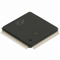
CY7C026AV-25AC Cypress Semiconductor Corp, CY7C026AV-25AC Datasheet

CY7C026AV-25AC
Specifications of CY7C026AV-25AC
Available stocks
Related parts for CY7C026AV-25AC
CY7C026AV-25AC Summary of contents
Page 1
... A –A for 8K devices BUSY is an output in master mode and an input in slave mode. Cypress Semiconductor Corporation Document #: 38-06052 Rev. *M CY7C024AV/024BV/025AV/026AV 3.3V 4K/8K/16K x 16/18 Dual-Port Fully asynchronous operation ■ Automatic power down ■ Expandable data bus to 32 bits, 36 bits or more using Master ■ ...
Page 2
Pin Configurations 100 10L 11L IO 12L 7 IO 13L 8 GND 14L IO 11 15L CY7C024AV/024BV (4K × 16 ...
Page 3
... GND 13 IO0R 14 IO1R 15 IO2R 16 VCC 17 IO3R 18 IO4R 19 IO5R 20 IO6R Notes the CY7C0251AV. 12L the CY7C0251AVC. 12R Document #: 38-06052 Rev. *M CY7C024AV/024BV/025AV/026AV Figure 2. 100-Pin TQFP (Top View CY7C0241AV (4K × 18) CY7C0251AV (8K × 18 CY7C026AV (16K × 16 CY7C0241AV/0251AV/036AV INT L 65 BUSY 64 L GND BUSY 61 R INT ...
Page 4
Pin Configurations (continued) 100 17L IO 5 11L IO 6 12L IO 13L 7 IO 14L 8 GND 15L IO 11 16L GND ...
Page 5
Pin Definitions Left Port Right Port R/W R –A A –A 0L 13L 0R 13R IO –IO IO –IO 0L 17L 0R 17R SEM SEM ...
Page 6
... CY7C024AV/024BV/41AV/1FFE for the CY7C025AV/51AV, 3FFE for the CY7C026AV/36AV) is the mailbox for the left port. When one port writes to the other port’s mailbox, an interrupt is generated to the owner. The interrupt is reset when the owner reads the contents of the mailbox. The message is user defined. Each port can read the other port’ ...
Page 7
Table 1. Non-Contending Read/Write Inputs CE R ...
Page 8
... OUT Notes 14. The voltage on any input or IO pin cannot exceed the power pin during power up. 15. Pulse width < 20 ns. 16. Industrial parts are available in CY7C026AV and CY7C036AV only. 17. VIL > –1.5V for pulse width less than 10ns. 18 1/t = All inputs cycling 1/t (except output enable) ...
Page 9
R1 = 590 OUTPUT 435 (a) Normal Load (Load 1) 3.0V GND Switching Characteristics [20] Over the Operating Range Parameter Read Cycle t Read Cycle Time RC t Address to Data Valid AA ...
Page 10
Switching Characteristics [20] Over the Operating Range (continued) Parameter t Write Pulse Width PWE t Data Setup to Write End SD t Data Hold From Write End HD [23, 24] t R/W LOW to High Z HZWE [23, 24] t ...
Page 11
Switching Waveforms Figure 5. Read Cycle No. 1 (Either Port Address Access) ADDRESS OHA DATA OUT PREVIOUS DATA VALID Figure 6. Read Cycle No. 2 (Either Port CE/OE Access) CE and DATA OUT ...
Page 12
Switching Waveforms (continued) Figure 8. Write Cycle No. 1: R/W Controlled Timing ADDRESS OE [38, 39 R/W NOTE 41 DATA OUT DATA IN Figure 9. Write Cycle No Controlled Timing ADDRESS [38, 39 ...
Page 13
Switching Waveforms (continued) Figure 10. Semaphore Read After Write Timing, Either Side A –A VALID ADRESS SEM R/W OE Figure 11. Timing Diagram of Semaphore Contention A – R/W L ...
Page 14
Switching Waveforms (continued) Figure 12. Timing Diagram of Read with BUSY (M/S=HIGH) ADDRESS R R/W R DATA ADDRESS L BUSY L DATA OUTL Figure 13. Write Timing with Busy Input (M/S=LOW) R/W BUSY Note 47. CE ...
Page 15
Switching Waveforms (continued) Figure 14. Busy Timing Diagram No.1 (CE Arbitration) CE Valid First L ADDRESS L BUSY R CE Valid First: R ADDRESS L BUSY L Figure 15. Busy Timing Diagram ...
Page 16
Switching Waveforms (continued) Left Side Sets INT : R ADDRESS WRITE 1FFF (OR 1/3FFF R/W L INT R [50] t INS Right Side Clears INT : R ADDRESS R INT R ...
Page 17
... CY7C024AV-25AXC CY7C024AV-25AXI 8K x16 3.3V Asynchronous Dual-Port SRAM Speed (ns) Ordering Code 20 CY7C025AV-20AXC 25 CY7C025AV-25AXC CY7C025AV-25AXI 16K x16 3.3V Asynchronous Dual-Port SRAM Speed (ns) Ordering Code 20 CY7C026AV-20AXC 25 CY7C026AV-25AC CY7C026AV-25AXC CY7C026AV-25AI CY7C026AV-25AXI Ordering Code Definitions Document #: 38-06052 Rev. *M CY7C024AV/024BV/025AV/026AV Package Diagram Package Type 51-85048 100-Pin Pb-Free Thin Quad Flat Pack ...
Page 18
Package Diagram Figure 17. 100-Pin Pb-Free Thin Plastic Quad Flat Pack (TQFP) A100 Document #: 38-06052 Rev. *M CY7C024AV/024BV/025AV/026AV CY7C0241AV/0251AV/036AV 51-85048 *E Page [+] Feedback ...
Page 19
... Added CY7C025AV-25AI to Ordering Information Removed cross information from features section Added CY7C024AV-25AI to Ordering Information Corrected x18 for 026AV to x16 Added Pb-free packaging information Corrected pin A113L to A13L on CY7C026AV pin list Added minimum V of 0.3V and note 16 IL Corrected CY7C024AC-25AXC to CY7C024AV-25AXC in Ordering Information ...
Page 20
... Cypress against all charges. Any Source Code (software and/or firmware) is owned by Cypress Semiconductor Corporation (Cypress) and is protected by and subject to worldwide patent protection (United States and foreign), United States copyright laws and international treaty provisions. Cypress hereby grants to licensee a personal, non-exclusive, non-transferable license to copy, use, modify, create derivative works of, and compile the Cypress Source Code and derivative works for the sole purpose of creating custom software and or firmware in support of licensee product to be used only in conjunction with a Cypress integrated circuit as specified in the applicable agreement ...


