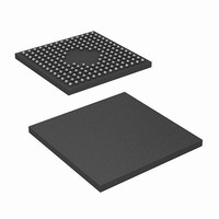
CY7C09569V-100BBC Cypress Semiconductor Corp, CY7C09569V-100BBC Datasheet - Page 12

CY7C09569V-100BBC
Manufacturer Part Number
CY7C09569V-100BBC
Description
IC,SYNC SRAM,16KX36,CMOS,BGA,172PIN,PLASTIC
Manufacturer
Cypress Semiconductor Corp
Datasheet
1.CY7C09579V-100AXC.pdf
(32 pages)
Specifications of CY7C09569V-100BBC
Format - Memory
RAM
Memory Type
SRAM - Dual Port, Synchronous
Memory Size
576K (16K x 36)
Speed
100MHz
Interface
Parallel
Voltage - Supply
3 V ~ 3.6 V
Operating Temperature
0°C ~ 70°C
Package / Case
172-LFBGA
Lead Free Status / RoHS Status
Contains lead / RoHS non-compliant
Available stocks
Company
Part Number
Manufacturer
Quantity
Price
Company:
Part Number:
CY7C09569V-100BBC
Manufacturer:
Cypress Semiconductor Corp
Quantity:
10 000
Switching Waveforms
Bank Select Pipelined Read
Left Port Write to Flow-Through Right Port Read
Notes
Document Number: 38-06054 Rev. *E
21. In this depth expansion example, B1 represents Bank #1 and B2 is Bank #2; Each Bank consists of one Cypress dual-port device from this data sheet.
22. B0 = B1 = B2 = B3 = BM = SIZE = ADS = CNTEN = V
23. The same waveforms apply for a right port write to flow-through left port read.
24. CE = B0 = B1 = B2 = B3 = ADS = CNTEN=V
25. OE = V
26. If t
Data
Data
Address
Address
ADDRESS
until t
Data
Address
Address
CCS
OUT(B2)
OUT(B1)
Data
CE
CE
CCS
CLK
CLK
R/W
CLK
R/W
maximum specified, then data from right port READ is not valid until the maximum specified for t
OUTR
IL
(B1)
(B1)
(B2)
(B2)
for the right port, which is being read from. OE = V
INL
+ t
(B1)
L
R
R
R
L
L
L
CD1
= ADDRESS
(t
t
t
t
t
SC
SC
SA
SA
CWDD
t
t
t
does not apply in this case).
SW
SD
SA
A
A
(B2)
0
0
t
CH2
.
Match
Valid
t
t
t
t
SW
SA
t
t
t
t
(continued)
CYC2
CCS
HA
HC
HA
HC
Match
[21, 22]
t
DC
t
CL2
t
t
t
HW
HA
t
t
HW
HA
HD
IL
; CNTRST= V
A
A
1
1
t
CWDD
t
IL
CD2
, CNTRST = V
t
CD1
IH
IH
t
.
for the left port, which is being written to.
SC
Q
t
0
SC
[22, 23, 24, 25, 26]
IH
A
.
A
2
2
t
t
DC
HC
t
HC
t
CD2
Match
No
Valid
Q
A
A
1
Match
3
t
3
No
DC
t
t
CKLZ
CKHZ
t
t
CD2
DC
CWDD
. If t
CCS
t
CD1
>maximum specified, then data is not valid
A
Q
A
4
2
4
t
t
t
CKHZ
CD2
CKLZ
Q
CY7C09569V
CY7C09579V
3
A
A
5
t
5
Valid
t
t
CKLZ
CKHZ
CD2
Page 12 of 32
Q
4
[+] Feedback


