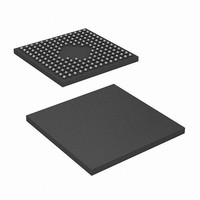
CY7C09569V-100BBC Cypress Semiconductor Corp, CY7C09569V-100BBC Datasheet - Page 26

CY7C09569V-100BBC
Manufacturer Part Number
CY7C09569V-100BBC
Description
IC,SYNC SRAM,16KX36,CMOS,BGA,172PIN,PLASTIC
Manufacturer
Cypress Semiconductor Corp
Datasheet
1.CY7C09579V-100AXC.pdf
(32 pages)
Specifications of CY7C09569V-100BBC
Format - Memory
RAM
Memory Type
SRAM - Dual Port, Synchronous
Memory Size
576K (16K x 36)
Speed
100MHz
Interface
Parallel
Voltage - Supply
3 V ~ 3.6 V
Operating Temperature
0°C ~ 70°C
Package / Case
172-LFBGA
Lead Free Status / RoHS Status
Contains lead / RoHS non-compliant
Available stocks
Company
Part Number
Manufacturer
Quantity
Price
Company:
Part Number:
CY7C09569V-100BBC
Manufacturer:
Cypress Semiconductor Corp
Quantity:
10 000
Word (18-bit) Operation
Word (18-bit) bus sizing operation is enabled when Bus Match
Select (BM) is set to a logic “1” and the Bus Size Select (SIZE)
pin is set to a logic “0.” In this mode, 18 bits of data are ported
through I/O
determines the right port data I/O sequencing order (Big Endian
or Little Endian).
During word (18-bit) bus size operation, a logic LOW applied to
the BE pin will select Little Endian operation. In this case, the
least significant data word is read from the right port first or
written to the right port first. A logic “1” on the BE pin during word
(18-bit) bus size operation will select Big Endian operation
resulting in the most significant data word being transferred
through the right port first. Internally, the data will be stored in the
appropriate 36-bit LSB or MSB I/O memory location. Device
operation requires a minimum of two clock cycles to read or write
during word (18-bit) bus size operation. An internal sub-counter
automatically increments the right port multiplexer control when
Little or Big Endian operation is in effect.
Document Number: 38-06054 Rev. *E
0R–17R
. The level applied to the Big Endian (BE) pin
Byte (9-bit) Operation
Byte (9-bit) bus sizing operation is enabled when Bus Match
Select (BM) is set to a logic “1” and the Bus Size Select (SIZE)
pin is set to a logic “1.” In this mode, 9 bits of data are ported
through I/O
Big Endian and Little Endian data sequencing is available for
dual-port operation. The level applied to the Big Endian pin (BE)
under these circumstances will determine the right port data I/O
sequencing order (Big or Little Endian). A logic LOW applied to
the BE pin during byte (9-bit) bus size operation will select Little
Endian operation. In this case, the least significant data byte is
read from the right port first or written to the right port first. A logic
“1” on the BE pin during byte (9-bit) bus size operation will select
Big Endian operation resulting in the most significant data word
to be transferred through the right port first. Internally, the data
will be stored in the appropriate 36-bit LSB or MSB I/O memory
location. Device operation requires a minimum of four clock
cycles to read or write during byte (9-bit) bus size operation. An
internal sub-counter automatically increments the right port
multiplexer control when Little or Big Endian operation is in
effect. When transferring data in byte (9-bit) bus match format,
the unused I/O pins (I/O
0R–8R
.
9RQ–35R
) are three-stated.
CY7C09569V
CY7C09579V
Page 26 of 32
[+] Feedback


