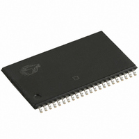
CY7C1020CV33-15ZSXE Cypress Semiconductor Corp, CY7C1020CV33-15ZSXE Datasheet

CY7C1020CV33-15ZSXE
Specifications of CY7C1020CV33-15ZSXE
Related parts for CY7C1020CV33-15ZSXE
CY7C1020CV33-15ZSXE Summary of contents
Page 1
... HIGH), the outputs are disabled (OE HIGH), the BHE and BLE are disabled (BHE, BLE HIGH), or during a write operation (CE LOW, and WE LOW). The CY7C1020CV33 is available in standard 44-pin TSOP Type II package. DATA IN DRIVERS 32K × 16 RAM Array COLUMN DECODER • ...
Page 2
... AC Test Loads and Waveforms ....................................... 6 Switching Characteristics ................................................ 6 Switching Waveforms ...................................................... 7 Read Cycle No. 1 ........................................................ 7 Read Cycle No. 2 (OE Controlled) .............................. 7 Write Cycle No. 1 (CE Controlled) ............................... 8 Document Number: 38-05133 Rev. *H CY7C1020CV33 Write Cycle No. 2 (BLE or BHE Controlled) ................ 8 Write Cycle No. 3 (WE Controlled, OE LOW) ............. 9 Truth Table ........................................................................ 9 Ordering Information ...................................................... 10 Ordering Code Definitions ......................................... 10 Package Diagrams .......................................................... 10 Acronyms ...
Page 3
... NC pins are not connected on the die. Document Number: 38-05133 Rev. *H –10 10 Commercial/Industrial 90 Automotive – Commercial/Industrial 5 Automotive – TSOP II Top View BHE BLE CE 6 I I I I/O I I/O I I/O I I/O I I/O I CY7C1020CV33 –12 –15 Unit – – Page [+] Feedback ...
Page 4
... When LOW, the I/O pins are allowed to behave as outputs. When deasserted HIGH, I/O pins are tri-stated, and act as input data pins. Ground Ground for the device. Should be connected to ground of the system. Power Supply Power Supply inputs to the device. CY7C1020CV33 Description –I ...
Page 5
... IN Test Conditions = 25 MHz Test Conditions Test conditions follow standard test methods and procedures for measuring thermal impedance, per EIA/JESD51. CY7C1020CV33 Ambient Temperature C to +70 C 3.3 V 10% –40 C to +85 C 3.3 V 10% –40 C to +125 C 3.3 V 10% – ...
Page 6
... HZCE LZCE HZOE LZOE HZWE CY7C1020CV33 High Z characteristics: R 317 3.3 V OUTPUT 351 (c) –12 –15 Unit Max Min Max 12 – 15 – ns – 12 – – 3 – ...
Page 7
... CURRENT Notes 9. Device is continuously selected. OE, CE, BHE and/or BHE = V 10 HIGH for Read cycle. 11. Address valid prior to or coincident with CE transition LOW. Document Number: 38-05133 Rev OHA t RC DATA VALID 50 CY7C1020CV33 DATA VALID t HZOE t HZCE t HZBE HIGH IMPEDANCE ICC CC 50% I ISB ...
Page 8
... Write Cycle No. 2 (BLE or BHE Controlled) ADDRESS t SA BHE, BLE WE CE DATA I/O Notes 12. Data I/O is high impedance BHE and/or BLE = V 13 goes HIGH simultaneously with WE going HIGH, the output remains in a high-impedance state. Document Number: 38-05133 Rev SCE PWE PWE t SCE CY7C1020CV33 Page [+] Feedback ...
Page 9
... Read—All bits High Z Read—Lower bits only Data out Read—Upper bits only Data in Write—All bits High Z Write—Lower bits only Data in Write—Upper bits only High Z Selected, outputs disabled High Z Selected, outputs disabled CY7C1020CV33 LZWE Mode Power Standby ( Active ( ...
Page 10
... Ordering Information Speed Ordering Code (ns) 15 CY7C1020CV33-15ZSXE CY7C1020CV33-15ZSXET Ordering Code Definitions CY7C 1020 C V33 - 15 ZSX E X Package Diagrams Figure 1. 44-pin TSOP II, 51-85087 Document Number: 38-05133 Rev. *H Package Diagram Package Type 51-85087 44-pin TSOP Type II (Pb-free) 51-85087 44-pin TSOP Type II (Pb-free Blank T = Tape and Reel ...
Page 11
... I/O input/output OE output enable SRAM static random access memory TSOP thin small-outline package TTL transistor-transistor logic WE write enable Document Number: 38-05133 Rev. *H CY7C1020CV33 Document Conventions Units of Measure Symbol Unit of Measure ns nano seconds V Volts µA micro Amperes mA milli Amperes mW milli Watts ...
Page 12
... Document History Page Document Title: CY7C1020CV33 512 K (32 K × 16) Static RAM Document Number: 38-05133 Orig. of REV. ECN NO. Issue Date Change ** 109428 12/16/01 *A 115045 05/30/02 *B 117615 08/14/02 *C 262949 See ECN *D 334398 See ECN *E 493543 See ECN *F 2897691 03/23/2010 *G 3057593 10/13/2010 *H 3100106 12/02/2010 Document Number: 38-05133 Rev ...
Page 13
... Cypress against all charges. Use may be limited by and subject to the applicable Cypress software license agreement. Document Number: 38-05133 Rev. *H All products and company names mentioned in this document may be the trademarks of their respective holders. cypress.com/go/plc Revised December 2, 2010 CY7C1020CV33 PSoC Solutions psoc.cypress.com/solutions PSoC 1 | PSoC 3 ...


