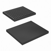
CY7C1380D-167BZC Cypress Semiconductor Corp, CY7C1380D-167BZC Datasheet - Page 10

CY7C1380D-167BZC
Manufacturer Part Number
CY7C1380D-167BZC
Description
CY7C1380D-167BZC
Manufacturer
Cypress Semiconductor Corp
Datasheet
1.CY7C1380D-167AXC.pdf
(34 pages)
Specifications of CY7C1380D-167BZC
Format - Memory
RAM
Memory Type
SRAM - Synchronous
Memory Size
18M (512K x 36)
Speed
167MHz
Interface
Parallel
Voltage - Supply
3.135 V ~ 3.6 V
Operating Temperature
0°C ~ 70°C
Package / Case
165-LFBGA
Lead Free Status / RoHS Status
Contains lead / RoHS non-compliant
Available stocks
Company
Part Number
Manufacturer
Quantity
Price
Company:
Part Number:
CY7C1380D-167BZC
Manufacturer:
CYPRESS
Quantity:
364
Company:
Part Number:
CY7C1380D-167BZC
Manufacturer:
Cypress Semiconductor Corp
Quantity:
10 000
Company:
Part Number:
CY7C1380D-167BZCT
Manufacturer:
Cypress Semiconductor Corp
Quantity:
10 000
Truth Table
The Truth Table for this data sheet follows.
Document #: 38-05543 Rev. *F
Notes
Deselect Cycle, Power Down
Deselect Cycle, Power Down
Deselect Cycle, Power Down
Deselect Cycle, Power Down
Deselect Cycle, Power Down
Sleep Mode, Power Down
READ Cycle, Begin Burst
READ Cycle, Begin Burst
WRITE Cycle, Begin Burst
READ Cycle, Begin Burst
READ Cycle, Begin Burst
READ Cycle, Continue Burst
READ Cycle, Continue Burst
READ Cycle, Continue Burst
READ Cycle, Continue Burst
WRITE Cycle, Continue Burst
WRITE Cycle, Continue Burst
READ Cycle, Suspend Burst
READ Cycle, Suspend Burst
READ Cycle, Suspend Burst
READ Cycle, Suspend Burst
WRITE Cycle, Suspend Burst
WRITE Cycle, Suspend Burst
4. X = Don't Care, H = Logic HIGH, L = Logic LOW.
5. WRITE = L when any one or more byte write enable signals, and BWE = L or GW = L. WRITE = H when all byte write enable signals, BWE, GW = H.
6. The DQ pins are controlled by the current cycle and the OE signal. OE is asynchronous and is not sampled with the clock.
7. The SRAM always initiates a read cycle when ADSP is asserted, regardless of the state of GW, BWE, or BW
8. OE is asynchronous and is not sampled with the clock rise. It is masked internally during write cycles. During a read cycle all data bits are tri-state when OE is
after the ADSP or with the assertion of ADSC . As a result, OE must be driven HIGH prior to the start of the write cycle to allow the outputs to tri-state. OE is a
don't care for the remainder of the write cycle.
inactive or when the device is deselected, and all data bits behave as output when OE is active (LOW) .
Operation
Add. Used
External
External
External
External
External
Current
Current
Current
Current
Current
Current
None
None
None
None
None
None
Next
Next
Next
Next
Next
Next
[4, 5, 6, 7, 8]
CE
H
X
X
X
H
H
X
H
X
X
H
H
X
H
L
L
L
L
L
L
L
L
L
1
CE
X
H
H
H
H
H
X
X
X
X
X
X
X
X
X
X
X
L
X
L
X
X
X
2
CE
X
X
H
X
H
X
L
X
X
X
X
X
X
X
X
X
X
X
X
L
L
L
L
3
ZZ ADSP ADSC
H
L
L
L
L
L
L
L
L
L
L
L
L
L
L
L
L
L
L
L
L
L
L
H
H
X
H
H
H
H
H
X
X
H
X
H
H
X
X
H
X
X
L
L
L
L
X
X
H
H
H
H
H
H
H
H
H
H
H
H
L
X
X
L
L
X
L
L
L
X
. Writes may occur only on subsequent clocks
ADV WRITE OE CLK
CY7C1380D, CY7C1382D
CY7C1380F, CY7C1382F
X
X
X
X
X
X
X
X
X
X
X
H
H
H
H
H
H
L
L
L
L
L
L
X
X
H
H
H
H
H
H
H
H
H
H
X
X
X
X
X
X
L
L
L
L
L
X
X
X
X
X
X
H
X
H
H
H
X
X
H
H
X
X
L
L
L
L
L
L
L-H
L-H
L-H
L-H
L-H
L-H
L-H
L-H
L-H
L-H
L-H
L-H
L-H
L-H
L-H
L-H
L-H
L-H
L-H
L-H
L-H
L-H
X
Page 10 of 34
Tri-State
Tri-State
Tri-State
Tri-State
Tri-State
Tri-State
Tri-State
Tri-State
Tri-State
Tri-State
Tri-State
Tri-State
DQ
Q
D
Q
Q
Q
D
D
Q
Q
D
D
[+] Feedback


