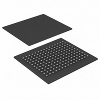
CY7C1460AV25-167BZXI Cypress Semiconductor Corp, CY7C1460AV25-167BZXI Datasheet - Page 11

CY7C1460AV25-167BZXI
Manufacturer Part Number
CY7C1460AV25-167BZXI
Description
CY7C1460AV25-167BZXI
Manufacturer
Cypress Semiconductor Corp
Datasheet
1.CY7C1460AV25-167BZC.pdf
(29 pages)
Specifications of CY7C1460AV25-167BZXI
Format - Memory
RAM
Memory Type
SRAM - Synchronous
Memory Size
36M (1M x 36)
Speed
167MHz
Interface
Parallel
Voltage - Supply
2.375 V ~ 2.625 V
Operating Temperature
-40°C ~ 85°C
Package / Case
165-LFBGA
Lead Free Status / RoHS Status
Lead free / RoHS Compliant
Available stocks
Company
Part Number
Manufacturer
Quantity
Price
Company:
Part Number:
CY7C1460AV25-167BZXI
Manufacturer:
Cypress Semiconductor Corp
Quantity:
10 000
Partial Write Cycle Description
Document Number: 38-05354 Rev. *G
Read
Write – no bytes written
Write byte a – (DQ
Write byte b – (DQ
Write bytes b, a
Write byte c – (DQ
Write bytes c, a
Write bytes c, b
Write bytes c, b, a
Write byte d – (DQ
Write bytes d, a
Write bytes d, b
Write bytes d, b, a
Write bytes d, c
Write bytes d, c, a
Write bytes d, c, b
Write all bytes
Read
Write – no bytes written
Write byte X(DQ
Write all bytes
Notes
8. X = “Don't Care”, H = Logic HIGH, L = Logic LOW, CE stands for all chip enables active. BWx = L signifies at least one byte write select is active, BWx = valid
9. Write is defined by WE and BW
10. When a write cycle is detected, all I/Os are tri-stated, even during byte writes.
11. Table only lists a partial listing of the byte write combinations. Any combination of BW
Read
Write – no bytes written
Write byte a – (DQ
Write byte b – (DQ
Write both bytes
signifies that the desired byte write selects are asserted, see Write Cycle Description table for details.
Function (CY7C1460AV25)
a
b
c
d
x
a
b
and DQP
and DQP
and DQP
and DQP
and DQP
Function (CY7C1462AV25)
Function (CY7C1464AV25)
and DQP
and DQP
X
. See Write Cycle Description table for details.
c
a
d
x)
b
)
)
)
a
b
)
)
)
[8, 9, 10, 11]
WE
H
L
L
L
L
L
L
L
L
L
L
L
L
L
L
L
L
X
is valid. Appropriate write will be done based on which byte write is active.
BW
X
H
H
H
H
H
H
H
H
L
L
L
L
L
L
L
L
d
WE
H
L
L
L
L
WE
BW
H
L
L
L
LL
H
H
H
H
H
H
H
H
X
L
L
L
L
L
L
L
c
BW
X
H
H
L
L
b
BW
X
H
H
H
H
H
H
H
H
L
L
L
L
L
L
L
L
CY7C1460AV25
CY7C1462AV25
CY7C1464AV25
b
All BW = L
BW
BW
H
H
H
X
X
L
L
L
Page 11 of 29
BW
a
x
X
H
H
H
H
H
H
H
H
L
L
L
L
L
L
L
L
a
[+] Feedback


