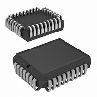
CY7C4261V-10JXC Cypress Semiconductor Corp, CY7C4261V-10JXC Datasheet - Page 6

CY7C4261V-10JXC
Manufacturer Part Number
CY7C4261V-10JXC
Description
IC,FIFO,16KX9,SYNCHRONOUS,CMOS,LDCC,32PIN,PLASTIC
Manufacturer
Cypress Semiconductor Corp
Series
CY7Cr
Datasheet
1.CY7C4281V-10JXC.pdf
(22 pages)
Specifications of CY7C4261V-10JXC
Function
Synchronous
Memory Size
144K (16K x 9)
Data Rate
100MHz
Access Time
8ns
Voltage - Supply
3.3V
Operating Temperature
-40°C ~ 85°C
Mounting Type
Surface Mount
Package / Case
32-PLCC
Lead Free Status / RoHS Status
Lead free / RoHS Compliant
Available stocks
Company
Part Number
Manufacturer
Quantity
Price
Company:
Part Number:
CY7C4261V-10JXC
Manufacturer:
CYPRESS
Quantity:
101
Company:
Part Number:
CY7C4261V-10JXC
Manufacturer:
Cypress Semiconductor Corp
Quantity:
135
Company:
Part Number:
CY7C4261V-10JXC
Manufacturer:
Cypress Semiconductor Corp
Quantity:
10 000
It is not necessary to write to all the offset registers at one time.
A subset of the offset registers can be written; then by bringing
the WEN2/LD input HIGH, the FIFO is returned to normal read
and write operation. The next time WEN2/LD is brought LOW, a
write operation stores data in the next offset register in
sequence.
The contents of the offset registers can be read to the data
outputs when WEN2/LD is LOW and both REN1 and REN2 are
LOW. LOW-to-HIGH transitions of RCLK read register contents
to the data outputs. Writes and reads should not be performed
simultaneously on the offset registers.
Programmable Flag (PAE, PAF) Operation
Whether the flag offset registers are programmed as described
in
almost-empty flag (PAE) and programmable almost-full flag
(PAF) states are determined by their corresponding offset
registers and the difference between the read and write pointers.
Table 2. Status Flags
Document #: 38-06013 Rev. *F
Notes
0
1 to n
(n + 1) to (1638 (m + 1)) (n + 1) to (32768 (m + 1)) (n + 1) to (65536 (m + 1)) (n + 1) to (131072 (m + 1))
(16384 m)
16384
1. The same selection sequence applies to reading from the registers. REN1 and REN2 are enabled and a read is performed on the LOW-to-HIGH transition of RCLK.
2. n = Empty Offset (n = 7 default value).
3. m = Full Offset (m = 7 default value).
Table 1
[2]
CY7C4261V
or the default values are used, the programmable
[3]
to 16383 (32768 m)
0
1 to n
32768
[2]
CY7C4271V
[3]
to 32767
Number of Words in FIFO
0
1 to n
(65536 m)
65536
[2]
CY7C4281V
[3]
to 65535
Table 1. Writing the Offset Registers
The number formed by the empty offset least significant bit
register and empty offset most significant bit register is referred
to as n and determines the operation of PAE. PAE is synchronized to
the LOW-to-HIGH transition of RCLK by one flip-flop and is LOW
when the FIFO contains n or fewer unread words. PAE is set
HIGH by the LOW-to-HIGH transition of RCLK when the FIFO
contains (n+1) or greater unread words.
The number formed by the full offset least significant bit register
and full offset most significant bit register is referred to as m and
determines the operation of PAF. PAF is synchronized to the
LOW-to-HIGH transition of WCLK by one flip-flop and is set LOW
when the number of unread words in the FIFO is greater than or
equal to CY7C4261V (16k – m), CY7C4271V (32k – m),
CY7C4281V (64k – m) and CY7C4291V (128k – m). PAF is set
HIGH by the LOW-to-HIGH transition of WCLK when the number
of available memory locations is greater than m.
LD
0
0
1
1
WEN
0
1
0
1
0
1 to n
(131072 m)
131072
[2]
WCLK
CY7C4291V
CY7C4261V/CY7C4271V
CY7C4281V/CY7C4291V
[3]
to 131071
No operation
Write into FIFO
No operation
Empty offset (LSB)
Empty offset (MSB)
Full offset (LSB)
Full offset (MSB)
[1]
Selection
FF PAF PAE EF
H
H
H
H
L
H
H
H
L
L
Page 6 of 22
H
H
H
L
L
H
H
H
H
L
[+] Feedback


