DAC1203D160HW/C1:5 NXP Semiconductors, DAC1203D160HW/C1:5 Datasheet
DAC1203D160HW/C1:5
Specifications of DAC1203D160HW/C1:5
935286681551
DAC1203D160HW/C1
DAC1203D160HW/C1-S
DAC1203D160HW/C1-S
Available stocks


Related parts for DAC1203D160HW/C1:5


DAC1203D160HW/C1:5 Summary of contents
Page 1
DAC1203D160 Dual 12 bits DAC 160 MHz interpolating Rev. 02 — 14 August 2008 1. General description The DAC1203D160 is optimized to reduce architecture complexity and overall system cost. The Digital-to-Analog Converter (DAC) leads dynamic performance ...
Page 2
... NXP Semiconductors 4. Ordering information Table 1. Ordering information Type number Package Name DAC1203D160HW HTQFP80 5. Block diagram (1) Pins 1, 3, 61, 65, 76 and 80. (2) Pins 4, 7, 62, 64, 66, 67, 70, 71, 74, 75, 77 and 79. (3) Pins 9, 17, 25, 29, 30, 35, 44, 49, 50, 52, 53, 54, 55 and 56. (4) Pins 18, 26, 36, 43, 63 and 78. ...
Page 3
... NXP Semiconductors 6. Pinning information 6.1 Pinning V CCA V CCA AGND CLK CLKN AGND DGND V CCD DGND DEC Fig 2. Pin configuration 6.2 Pin description Table 2. Symbol V CCA i.c. V CCA AGND CLK CLKN AGND i.c. DGND DAC1203D160_2 Product data sheet Dual 12 bits DAC 160 MHz interpolating ...
Page 4
... NXP Semiconductors Table 2. Symbol V CCD I11 I10 DGND DEC DGND DEC n.c. n.c. DGND DGND Q11 Q10 Q9 Q8 DGND DEC DEC DGND Q1 Q0 n.c. n.c. DGND DGND DAC1203D160_2 Product data sheet Dual 12 bits DAC 160 MHz interpolating Pin description …continued [1] Pin ...
Page 5
... NXP Semiconductors Table 2. Symbol V CCD DGND DGND DGND DGND DGND GAPD GAPOUT QVIRES IVIRES V CCA AGND DEC AGND V CCA AGND AGND QOUTN QOUT AGND AGND IOUTN IOUT AGND AGND V CCA AGND DEC AGND V CCA [1] Type description: S: Supply; G: Ground; I: Input; O: Output. DAC1203D160_2 ...
Page 6
... NXP Semiconductors 7. Functional description The DAC1203D160 is a segmented architecture composed of a 7-bit thermometer sub-DAC and the remaining 5-bit in a binary weighted sub-DAC. The device produces two complementary current outputs on both channels, respectively pins IOUT/IOUTN and QOUT/QOUTN which need to be connected via a load resistor to the ground ...
Page 7
... NXP Semiconductors 8. Limiting values Table 3. In accordance with the Absolute Maximum Rating System (IEC 60134). Symbol V CCD V CCA stg T amb T j [1] All supplies are connected together. 9. Thermal characteristics Table 4. Symbol R th(j-a) R th(c-a) DAC1203D160_2 Product data sheet Dual 12 bits DAC 160 MHz interpolating ...
Page 8
... NXP Semiconductors 10. Characteristics Table 5. Characteristics 3 3.6 V; AGND and DGND connected together; T CCD CCA 3 and T CCD CCA O(fs) Figure 10; unless otherwise specified. Symbol Parameter Supplies V digital supply voltage CCD V analog supply voltage CCA I digital supply current CCD I analog supply current CCA ...
Page 9
... NXP Semiconductors Table 5. Characteristics …continued 3 3.6 V; AGND and DGND connected together; T CCD CCA 3 and T CCD CCA O(fs) Figure 10; unless otherwise specified. Symbol Parameter Digital filter specification (FIR); Order N = 42; see f data rate data pass-band ripple ripple(pb) stop-band attenuation stpb ...
Page 10
... NXP Semiconductors Table 5. Characteristics …continued 3 3.6 V; AGND and DGND connected together; T CCD CCA 3 and T CCD CCA O(fs) Figure 10; unless otherwise specified. Symbol Parameter Signal-to-noise ratio NSD noise spectral density S/N signal-to-noise ratio ACPR adjacent channel power ratio [1] Guaranteed by design. Table 6. ...
Page 11
... NXP Semiconductors 20 output (dB 100 140 180 0 0.2 0.4 normalized frequency f Fig 6. FIR filter frequency response Table 7. Coefficient H(1) H(2) H(3) H(4) H(5) H(6) H(7) H(8) H(9) H(10) H(11) H(12) H(13) H(14) H(15) H(16) H(17) H(18) H(19) H(20) H(21) H(22) DAC1203D160_2 ...
Page 12
... NXP Semiconductors 11. Application information R s CLK V CCA 1 k CLKN 100 AGND 004aaa547 Fig 8. Single-ended clock schematic DAC1203D160_2 Product data sheet Dual 12 bits DAC 160 MHz interpolating DAC1203D160 V Fig 9. Differential clock schematic Rev. 02 — 14 August 2008 DAC1203D160 AGND DAC1203D160 1 k CLK 100 nF ...
Page 13
... NXP Semiconductors AGND 3 CCA 1 3 CCA 3 3 AGND AGND 4 CLK 5 CLKN 6 AGND AGND 7 i.c. 8 DGND DGND CCD 10 3.3 V I11 11 I10 DGND DGND 17 C DEC All resistors are 1 % precision resistors 100 nF. Fig 10. Application diagram DAC1203D160_2 Product data sheet Dual 12 bits DAC 160 MHz interpolating ...
Page 14
... NXP Semiconductors 11.1 Alternative parts The following alternative parts are also available: Table 8. Type number DAC1403D160 DAC1003D160 [1] Pin to pin compatible DAC1203D160_2 Product data sheet Dual 12 bits DAC 160 MHz interpolating Alternative parts Description Dual 14 bits DAC Dual 10 bits DAC Rev. 02 — 14 August 2008 ...
Page 15
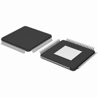
... NXP Semiconductors 12. Package outline HTQFP80: plastic thermal enhanced thin quad flat package; 80 leads; body mm; exposed die pad y exposed die pad pin 1 index DIMENSIONS (mm are the original dimensions) A UNIT max 0.15 1.05 0.27 mm 1.2 0.25 0.05 0.95 0.17 Note 1. Plastic or metal protrusions of 0.25 mm maximum per side are not included ...
Page 16
... NXP Semiconductors 13. Abbreviations Table 9. Acronym FIR IF LSB MSB PLL PMOS 14. Glossary 14.1 Static parameters DNL — Differential Non-Linearity. The difference between the ideal and the measured output value between successive DAC codes. INL — Integral Non-Linearity. The deviation of the transfer function from a best-fit straight line (linear regression computation) ...
Page 17
... NXP Semiconductors 15. Revision history Table 10. Revision history Document ID Release date DAC1203D160_2 20080814 • Modifications: Corrections to values in • Addition to description of row Q0 in • Corrections to row sequence in • Corrections to n.c pins in DAC1203D160_1 20080613 DAC1203D160_2 Product data sheet Dual 12 bits DAC 160 MHz interpolating ...
Page 18
... Right to make changes — NXP Semiconductors reserves the right to make changes to information published in this document, including without limitation specifications and product descriptions, at any time and without notice ...
Page 19
... NXP Semiconductors 18. Contents 1 General description . . . . . . . . . . . . . . . . . . . . . . 1 2 Features . . . . . . . . . . . . . . . . . . . . . . . . . . . . . . . 1 3 Applications . . . . . . . . . . . . . . . . . . . . . . . . . . . . 1 4 Ordering information . . . . . . . . . . . . . . . . . . . . . 2 5 Block diagram . . . . . . . . . . . . . . . . . . . . . . . . . . 2 6 Pinning information . . . . . . . . . . . . . . . . . . . . . . 3 6.1 Pinning . . . . . . . . . . . . . . . . . . . . . . . . . . . . . . . 3 6.2 Pin description . . . . . . . . . . . . . . . . . . . . . . . . . 3 7 Functional description . . . . . . . . . . . . . . . . . . . 6 8 Limiting values Thermal characteristics Characteristics . . . . . . . . . . . . . . . . . . . . . . . . . . 8 11 Application information 11.1 Alternative parts . . . . . . . . . . . . . . . . . . . . . . . 14 12 Package outline . . . . . . . . . . . . . . . . . . . . . . . . 15 13 Abbreviations ...