DG406DN-T1-E3 Vishay, DG406DN-T1-E3 Datasheet
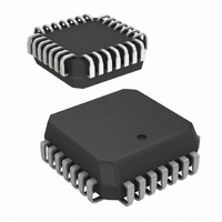
IC,ANALOG MUX,SINGLE,16-CHANNEL,CMOS,LDCC,28PIN,PLASTIC

DG406DN-T1-E3

Manufacturer Part Number
DG406DN-T1-E3
Description
IC,ANALOG MUX,SINGLE,16-CHANNEL,CMOS,LDCC,28PIN,PLASTIC
Manufacturer
Vishay
Datasheet

Specifications of DG406DN-T1-E3

Function
Multiplexer
Circuit
1 x 16:1
On-state Resistance
120 Ohm
Voltage Supply Source
Single, Dual Supply
Voltage - Supply, Single/dual (±)
12V, ±5 V ~ 20 V
Current - Supply
50µA
Operating Temperature
-40°C ~ 85°C
Mounting Type
Surface Mount
Package / Case
28-PLCC
Number Of Channels
16 Channel
On Resistance (max)
120 Ohms
Propagation Delay Time
350 ns
On Time (max)
600 ns
Off Time (max)
300 ns
Supply Voltage (max)
20 V
Supply Voltage (min)
5 V
Supply Current
0.05 mA
Maximum Power Dissipation
450 mW
Maximum Operating Temperature
+ 85 C
Minimum Operating Temperature
- 40 C
Mounting Style
SMD/SMT
Off State Leakage Current (max)
40 nA
Lead Free Status / RoHS Status
Lead free / RoHS Compliant
Lead Free Status / RoHS Status
Lead free / RoHS Compliant
Other names
DG406DN-T1-E3TR

Available stocks

Company
Part Number
Manufacturer
Quantity
Price
Part Number:
DG406DN-T1-E3
Manufacturer:
TI
Quantity:
114
Part Number:
DG406DN-T1-E3
Manufacturer:
Vishay Siliconix
Quantity:
10 000
Company:
Part Number:
DG406DN-T1-E3
Quantity:
8 000
DESCRIPTION
The DG406 is a 16 channel single-ended analog multiplexer
designed to connect one of sixteen inputs to a common
output as determined by a 4-bit binary address. The DG407
selects one of eight differential inputs to a common
differential output. Break-before-make switching action
protects against momentary shorting of inputs.
An on channel conducts current equally well in both
directions. In the off state each channel blocks voltages up
to the power supply rails. An enable (EN) function allows the
user to reset the multiplexer/demultiplexer to all switches off
for stacking several devices. All control inputs, address (A
and enable (EN) are TTL compatible over the full specified
operating temperature range.
Applications for the DG406, DG407 include high speed data
acquisition, audio signal switching and routing, ATE
systems, and avionics. High performance and low power
dissipation make them ideal for battery operated and remote
instrumentation applications.
Designed in the 44 V silicon-gate CMOS process, the
absolute maximum voltage rating is extended to 44 V,
allowing operation with ± 20 V supplies. Additionally single
(12 V) supply operation is allowed. An epitaxial layer
prevents latchup.
For applications information please request documents
70601 and 70604.
FUNCTIONAL BLOCK DIAGRAM AND PIN CONFIGURATION
* Pb containing terminations are not RoHS compliant, exemptions may apply
Document Number: 70061
S11-0179-Rev. J, 07-Feb-11
DG406
16-Ch/Dual 8-Ch High-Performance CMOS Analog Multiplexers
GND
S
S
S
S
S
S
S
NC
NC
NC
V+
S
A
16
15
14
13
12
10
11
9
3
Dual-In-Line and SOIC Wide-Body
10
12
13
14
11
1
2
3
4
5
6
7
8
9
Decoders/Drivers
Top View
28
27
26
25
24
23
22
21
20
19
18
17
16
15
D
V-
S
S
S
S
S
S
S
S
EN
A
A
A
8
7
6
5
4
3
2
1
0
1
2
x
)
FEATURES
BENEFITS
APPLICATIONS
• Low on-resistance - R
• Low charge injection - Q: 15 pC
• Fast transition time - t
• Low power: 0.2 mW
• Single supply capability
• Higher accuracy
• Reduced glitching
• Improved data throughput
• Reduced power consumption
• Increased ruggedness
• Wide supply ranges: ± 5 V to ± 20 V
• Data acquisition systems
• Audio signal routing
• Medical instrumentation
• ATE systems
• Battery powered systems
• High-rel systems
• Single supply systems
44 V supply max. rating
DG407
GND
S
S
S
S
S
S
S
S
NC
NC
NC
V+
D
8b
7b
6b
5b
4b
3b
2b
1b
b
Dual-In-Line and SOIC Wide-Body
10
11
12
13
14
1
2
3
4
5
6
7
8
9
TRANS
DS(on)
Decoders/Drivers
Top View
: 50 
: 200 ns
DG406, DG407
Vishay Siliconix
2
www.vishay.com
28
27
26
25
24
23
22
21
20
19
18
17
16
15
RoHS*
COMPLIANT
D
V-
S
S
S
S
S
S
S
S
EN
A
A
A
8a
7a
6a
5a
4a
3a
2a
1a
0
1
2
a
Available
Pb-free
1

Related parts for DG406DN-T1-E3

DG406DN-T1-E3 Summary of contents

Page 1

... Audio signal routing • Medical instrumentation • ATE systems • Battery powered systems • High-rel systems • Single supply systems DG407 Dual-In-Line and SOIC Wide-Body GND DG406, DG407 Vishay Siliconix : 50  DS(on) Pb-free Available : 200 ns TRANS RoHS* COMPLIANT Decoders/Drivers Top View www.vishay.com 1 ...

Page 2

... TRUTH TABLE (DG407 Switch 2 0 None Logic “0” Logic “1” not Care ORDERING INFORMATION (DG407) Part Number Temp. Range DG406DJ DG406DJ-E3 DG406DN - 40 ° °C DG406DN-T1-E3 DG406DW DG406DW-E3 PLCC and LCC Decoders/Drivers Top View Switch Pair None 0 2.4 V ...

Page 3

... All leads soldered or welded to PC board. c. Derate 6 mW/°C above 75°C. d. Derate 12 mW/°C above 75°C. e. Derate 13.5 mW/°C above 75°C . Document Number: 70061 S11-0179-Rev. J, 07-Feb- DG406, DG407 Vishay Siliconix Limit mA, whichever occurs first 30 100 - 65 to 150 - 65 to 125 625 1 ...

Page 4

... DG406, DG407 Vishay Siliconix a SPECIFICATIONS Parameter Symbol Analog Switch e Analog Signal Range V ANALOG Drain-Source R DS(on) On-Resistance R Matching Between R DS(on) g DS(on) Channels Source Off Leakage Current I S(off) Drain Off Leakage Current I D(off) Drain On Leakage Current I D(on) Digital Control Logic High Input Voltage ...

Page 5

... V Room Room INH INL Room nF Room Room Full Room Full DG406, DG407 Vishay Siliconix A Suffix D Suffix - 55 °C to 125 ° ° ° Typ. Min. Max. Min. Max 120 120 5 0.01 0.04 0.04 0.04 0.04 300 450 450 250 600 600 ...

Page 6

... DG406, DG407 Vishay Siliconix TYPICAL CHARACTERISTICS (T 160 120 80 ± ± ± ± ± Drain Voltage ( vs. V and Supply DS(on) D 240 V+ = 7.5 V 200 160 10 V 120 Drain Voltage ( vs. V and Supply DS(on) D 100 " D(on) D(of f) 100 0 Temperature (° Leakages vs. Temperature D S www.vishay.com ° ...

Page 7

... Off-Isolation vs. Frequency 300 260 220 t TRA 180 ON(E N) 140 100 t OFF Temperature (° vs. Temperature ON OFF Document Number: 70061 S11-0179-Rev. J, 07-Feb- °C, unless otherwise noted 100K 1M 10M 65 85 105 125 DG406, DG407 Vishay Siliconix Source Voltage (V) S Charge Injection vs. Analog Voltage 100 ...

Page 8

... DG406, DG407 Vishay Siliconix SCHEMATIC DIAGRAM (Typical Channel GND REF TEST CIRCUITS + 2 DG406 GND V- Ω Ω 50 300 - 2 DG407 GND V- Ω Ω 50 300 - ± www.vishay.com 8 Level Decode/ Shift Drive Figure 1. ± ± Logic Input Switch Output V O ± ± Figure 2. Transition Time ...

Page 9

... A 3 DG406 A 2 DG407 D GND V- 50 Ω 300 Ω Document Number: 70061 S11-0179-Rev. J, 07-Feb- Logic 35 pF Input Switch Output - Figure 3. Enable Switching Time Logic Input + Switch Output Figure 4. Break-Before-Make Interval DG406, DG407 Vishay Siliconix t < < ON(EN) OFF(EN < < OPEN 0 V www.vishay.com 9 ...

Page 10

... Figure 6. Measuring low-level analog signals is more accurate when using a differential multiplexing technique Vishay Siliconix maintains worldwide manufacturing capability. Products may be manufactured at one of several qualified locations. Reliability data for Silicon Technology and Package Reliability represent a composite of all qualified locations. For related documents such as package/tape drawings, part marking, and reliability data, see www ...

Page 11

... Vishay product could result in personal injury or death. Customers using or selling Vishay products not expressly indicated for use in such applications their own risk and agree to fully indemnify and hold Vishay and its distributors harmless from and against any and all claims, liabilities, expenses and damages arising or resulting in connection with such use or sale, including attorneys fees, even if such claim alleges that Vishay or its distributor was negligent regarding the design or manufacture of the part ...

Related keywords