DG604EQ-T1-E3 Vishay, DG604EQ-T1-E3 Datasheet - Page 4
DG604EQ-T1-E3
Manufacturer Part Number
DG604EQ-T1-E3
Description
1.0pC Charge Injection, 4-CH MUX
Manufacturer
Vishay
Datasheet
1.DG604EQ-T1-E3.pdf
(10 pages)
Specifications of DG604EQ-T1-E3
Function
Multiplexer
Circuit
2 x 1:1
On-state Resistance
160 Ohm
Current - Supply
1µA
Operating Temperature
-40°C ~ 125°C
Mounting Type
Surface Mount
Package / Case
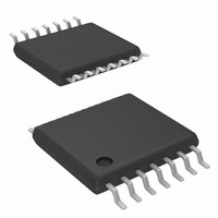
14-TSSOP
Number Of Channels
1 Channel
On Resistance (max)
245 Ohm @ 3 V
On Time (max)
108 ns @ 3 V
Off Time (max)
76 ns @ 3 V
Supply Voltage (max)
12 V
Supply Voltage (min)
2.7 V
Maximum Power Dissipation
450 mW
Maximum Operating Temperature
+ 125 C
Minimum Operating Temperature
- 40 C
Mounting Style
SMD/SMT
Number Of Switches
Single
Off Isolation (typ)
- 60 dB
Switch Current (typ)
0.000001 mA @ 5 V
Lead Free Status / RoHS Status
Lead free / RoHS Compliant
Lead Free Status / RoHS Status
Lead free / RoHS Compliant
Other names
DG604EQ-T1-E3TR
Available stocks
Company
Part Number
Manufacturer
Quantity
Price
Company:

Part Number:
DG604EQ-T1-E3
Manufacturer:
Vishay
Quantity:
23 772


DG604
Vishay Siliconix
www.vishay.com
4
SPECIFICATIONS FOR SINGLE SUPPLY
Parameter
Analog Switch
Analog Signal Range
On-Resistance
On-Resistance Match
Switch Off Leakage Current
(for 14 pin TSSOP)
Channel On Leakage Current
(for 14 pin TSSOP)
Switch Off
Leakage Current
(for 16 pin miniQFN)
Channel On
Leakage Current
(for 16 pin miniQFN)
Digital Control
Input Current, V
Input Current, V
Input Capacitance
Dynamic Characteristics
Transition Time
Enable Turn-On Time
Enable Turn-Off Time
Break-Before-Make-Time
Charge Injection
Off-Isolation
Crosstalk
Bandwidth
Total Harmonic Distortion
Source Off Capacitance
Drain Off Capacitance
Channel On Capacitance
Power Supplies
Power Supply Current
Negative Supply Current
Ground Current
e
e
e
IN
IN
Low
High
e
e
e
e
V
Symbol
t
R
t
t
OFF(EN)
ANALOG
C
C
ON(EN)
X
C
ΔR
TRANS
OIRR
I
I
I
I
I
I
t
THD
I
DS(on)
S(off)
D(off)
D(on)
S(off)
D(off)
D(on)
C
BMM
BW
GND
TALK
S(off)
D(off)
D(on)
I
Q
I+
I
I-
H
L
IN
ON
V
C
V
Signal = 1 V
f = 10 MHz, R
IN A0, A1 and ENABLE
L
S(CLOSE)
Unless Otherwise Specified
V
V
= 1 nF, R
D
D
I
I
R
= 1 V/4.5 V, V
= 1 V/4.5 V, V
V+ = 5.5 V, V- = - 5.5 V
S
S
V
V
V
V+ = 5.5 V, V- = 0 V,
V
L
V+ = 5.5 V, V- = 0 V
V+ = 5.5 V, V- = 0 V
Under Test = 0.8 V
Under Test = 2.0 V
= 1 mA, V
= 1 mA, V
IN A0, A1 and ENABLE
IN A0, A1 and ENABLE
Test Conditions
V+ = 5 V, V- = 0 V
S
S
= 300 Ω, C
V
= V
= V
= 3 V, V
IN
R
GEN
R
f = 1 MHz
f = 1 MHz
RMS,
L
= 0 V, or V+
L
D
D
L
New Product
= 600 Ω
= 50 Ω
= 1 V/4.5 V
= 1 V/4.5 V
= 50 Ω, C
= 0 Ω, V
20 Hz to 20 kHz,
D
D
S(OPEN)
S
S
L
= + 3.5 V
= + 3.5 V
= 2.0 V, 0.8 V
= 4.5 V/1 V
= 35 pF
= 4.5 V/1 V
GEN
L
= 0.0 V,
= 5 pF
= 0 V
a
Temp.
Room
Room
Room
Room
Room
Room
Room
Room
Room
Room
Room
Room
Room
Room
Room
Room
Room
Room
Room
Room
Room
Full
Full
Full
Full
Full
Full
Full
Full
Full
Full
Full
Full
Full
Full
Full
Full
Full
Full
Full
b
- 0.001
- 0.001
± 0.01
± 0.01
± 0.01
± 0.01
± 0.01
± 0.01
0.005
0.005
0.009
0.001
Typ.
0.15
11.6
16.2
- 58
- 81
120
330
4.3
3.1
36
30
17
23
3
c
- 40 °C to 125 °C - 40 °C to 85 °C
Min.
- 0.1
- 0.1
- 0.1
- 0.1
- 0.1
- 0.5
- 0.5
- 18
- 18
- 18
- 18
- 18
- 18
- 1
- 1
- 1
- 1
- 1
5
d
Max.
170
250
120
102
0.1
0.1
0.1
0.1
0.1
0.5
12
18
18
18
18
18
18
75
70
47
88
S09-0280-Rev. B, 16-Feb-09
5
5
1
1
1
1
Document Number: 69934
d
Min.
- 0.1
- 0.5
- 0.1
- 0.5
- 0.1
- 0.5
- 0.1
- 0.1
- 0.5
- 0.5
- 1
- 2
- 1
- 2
- 1
- 2
- 1
- 1
5
d
Max.
170
200
0.1
0.5
0.1
0.5
0.1
0.5
0.1
0.1
0.5
10
75
95
70
80
47
63
5
5
1
2
1
2
1
2
1
d
MHz
Unit
µA
pC
µA
nA
pF
dB
pF
ns
%
V
Ω
Related parts for DG604EQ-T1-E3
Image
Part Number
Description
Manufacturer
Datasheet
Request
R

Part Number:
Description:
Dg604 - 1.0 Pc Charge Injection, 100 Pa Leakage, 4-channel Multiplexer - Vishay Analog Switches And Multiplexers
Manufacturer:
Vishay
Datasheet:
Part Number:
Description:
357-036-542-201 CARDEDGE 36POS DL .156 BLK LOPRO
Manufacturer:
Vishay
Datasheet:
Part Number:
Description:
357-036-542-201 CARDEDGE 36POS DL .156 BLK LOPRO
Manufacturer:
Vishay
Datasheet:
Part Number:
Description:
357-036-542-201 CARDEDGE 36POS DL .156 BLK LOPRO
Manufacturer:
Vishay
Datasheet:
Part Number:
Description:
357-036-542-201 CARDEDGE 36POS DL .156 BLK LOPRO
Manufacturer:
Vishay
Datasheet:
Part Number:
Description:
357-036-542-201 CARDEDGE 36POS DL .156 BLK LOPRO
Manufacturer:
Vishay
Datasheet:
Part Number:
Description:
357-036-542-201 CARDEDGE 36POS DL .156 BLK LOPRO
Manufacturer:
Vishay
Datasheet:
Part Number:
Description:
357-036-542-201 CARDEDGE 36POS DL .156 BLK LOPRO
Manufacturer:
Vishay
Datasheet:
Part Number:
Description:
357-036-542-201 CARDEDGE 36POS DL .156 BLK LOPRO
Manufacturer:
Vishay
Datasheet:
Part Number:
Description:
357-036-542-201 CARDEDGE 36POS DL .156 BLK LOPRO
Manufacturer:
Vishay
Datasheet:
Part Number:
Description:
357-036-542-201 CARDEDGE 36POS DL .156 BLK LOPRO
Manufacturer:
Vishay
Datasheet:
Part Number:
Description:
357-036-542-201 CARDEDGE 36POS DL .156 BLK LOPRO
Manufacturer:
Vishay
Datasheet:
Part Number:
Description:
357-036-542-201 CARDEDGE 36POS DL .156 BLK LOPRO
Manufacturer:
Vishay
Datasheet:
Part Number:
Description:
357-036-542-201 CARDEDGE 36POS DL .156 BLK LOPRO
Manufacturer:
Vishay
Datasheet:
Part Number:
Description:
357-036-542-201 CARDEDGE 36POS DL .156 BLK LOPRO
Manufacturer:
Vishay
Datasheet: