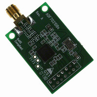
EVAL-ADF7021-NDBZ5 Analog Devices Inc, EVAL-ADF7021-NDBZ5 Datasheet - Page 39
EVAL-ADF7021-NDBZ5
Manufacturer Part Number
EVAL-ADF7021-NDBZ5
Description
Matching Unpopulated
Manufacturer
Analog Devices Inc
Type
Transceiver, FSKr
Datasheet
1.ADF7021-NBCPZ-RL.pdf
(64 pages)
Specifications of EVAL-ADF7021-NDBZ5
Frequency
80MHz ~ 650MHz
Lead Free Status / RoHS Status
Lead free / RoHS Compliant
For Use With/related Products
ADF7021-N
Lead Free Status / Rohs Status
Supplier Unconfirmed


When to Use a Fine Calibration
In cases where the receive signal bandwidth is very close to the
bandwidth of the IF filter, it is recommended to perform a fine
filter calibration every time the unit powers up in receive mode.
A fine calibration should be performed if
where:
OBW is the 99% occupied bandwidth of the transmit signal.
Coarse Calibration Variation is 2.5 kHz.
IF_FILTER_BW is set by R4_DB[30:31].
The FILTER_CAL_COMPLETE signal from MUXOUT (set by
R0_DB[29:31]) can be used to monitor the filter calibration
duration or to signal the end of calibration. A coarse filter
calibration is automatically performed prior to a fine filter
calibration.
When to Use Single Fine Calibration
In applications where the receiver powers up numerous times in
a short period, it is only necessary to perform a one-time fine
calibration on the initial receiver power-up.
After the initial coarse calibration and fine calibration, the result of
the fine calibration can be read back through the serial interface
using the FILTER_CAL_READBACK result (refer to the Filter
Bandwidth Calibration Readback section). On subsequent
power-ups in receive mode, the filter is manually adjusted using
the previous fine filter calibration result. This manual adjust is
performed using the IF_FILTER_ADJUST bits (R5_DB[14:19]).
This method should only be used if the successive power-ups in
receive mode are over a short duration, during which time there
is little variation in temperature (<15°C).
IF Filter Variation with Temperature
When calibrated, the filter center frequency can vary with changes
in temperature. If the ADF7021-N is used in an application where
it remains in receive mode for a considerable length of time, the
user must consider this variation of filter center frequency with
temperature. This variation is typically 1 kHz per 20°C, which
means that if a coarse filter calibration and fine filter calibration
are performed at 25°C, the initial maximum error is ±0.5 kHz,
and the maximum possible change in the filter center frequency
over temperature (−40°C to +85°C) is ±3.25 kHz. This gives a
total error of ±3.75 kHz.
If the receive signal occupied bandwidth is considerably less
than the IF filter bandwidth, the variation of filter center
frequency over the operating temperature range may not be
an issue. Alternatively, if the IF filter bandwidth is not wide
enough to tolerate the variation with temperature, a periodic
filter calibration can be performed or, alternatively, the on-chip
temperature sensor can be used to determine when a filter cali-
bration is necessary by monitoring for changes in temperature.
OBW + Coarse Calibration Variation > IF_FILTER_BW
Rev. 0 | Page 39 of 64
LNA/PA MATCHING
The ADF7021-N exhibits optimum performance in terms of
sensitivity, transmit power, and current consumption, only if its
RF input and output ports are properly matched to the antenna
impedance. For cost-sensitive applications, the ADF7021-N is
equipped with an internal Rx/Tx switch that facilitates the use
of a simple, combined passive PA/LNA matching network.
Alternatively, an external Rx/Tx switch such as the
be used, which yields a slightly improved receiver sensitivity
and lower transmitter power consumption.
Internal Rx/Tx Switch
Figure 50 shows the ADF7021-N in a configuration where
the internal Rx/Tx switch is used with a combined LNA/PA
matching network. This is the configuration used on the EVAL-
ADF7021-NDBxx evaluation board. For most applications, the
slight performance degradation of 1 dB to 2 dB caused by the
internal Rx/Tx switch is acceptable, allowing the user to take
advantage of the cost saving potential of this solution. The
design of the combined matching network must compensate for
the reactance presented by the networks in the Tx and the Rx
paths, taking the state of the Rx/Tx switch into consideration.
The procedure typically requires several iterations until an
acceptable compromise has been reached. The successful imple-
mentation of a combined LNA/PA matching network for the
ADF7021-N is critically dependent on the availability of an
accurate electrical model for the PCB. In this context, the use of a
suitable CAD package is strongly recommended. To avoid this
effort, a small form-factor reference design for the ADF7021-N is
provided, including matching and harmonic filter components.
The design is on a 2-layer PCB to minimize cost. Gerber files
are available at www.analog.com.
ANTENNA
BPF OR LPF
OPTIONAL
Figure 50. ADF7021-N with Internal Rx/Tx Switch
C1
C
C
A
B
V
BAT
L
L1
Z
Z
Z
A
IN
IN
OPT
_RFIN
_RFIN
_PA
ADF7021-N
PA_OUT
RFIN
RFINB
ADF7021-N
ADG919
LNA
PA
can
Related parts for EVAL-ADF7021-NDBZ5
Image
Part Number
Description
Manufacturer
Datasheet
Request
R

Part Number:
Description:
±1.7g Dual-Axis IMEMS Accelerometer Evaluation Board
Manufacturer:
Analog Devices Inc
Datasheet:

Part Number:
Description:
Inertial Sensor Evaluation System
Manufacturer:
Analog Devices Inc
Datasheet:
Part Number:
Description:
Manufacturer:
Analog Devices Inc
Datasheet:
Part Number:
Description:
Manufacturer:
Analog Devices Inc
Datasheet:
Part Number:
Description:
Manufacturer:
Analog Devices Inc
Datasheet:
Part Number:
Description:
Manufacturer:
Analog Devices Inc
Datasheet:
Part Number:
Description:
Manufacturer:
Analog Devices Inc
Datasheet:
Part Number:
Description:
Manufacturer:
Analog Devices Inc
Datasheet:
Part Number:
Description:
Manufacturer:
Analog Devices Inc
Datasheet:
Part Number:
Description:
Manufacturer:
Analog Devices Inc
Datasheet:
Part Number:
Description:
Manufacturer:
Analog Devices Inc
Datasheet:
Part Number:
Description:
Manufacturer:
Analog Devices Inc
Datasheet:
Part Number:
Description:
Manufacturer:
Analog Devices Inc
Datasheet: