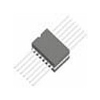
JM38510/11201BDA National Semiconductor, JM38510/11201BDA Datasheet - Page 6

JM38510/11201BDA
Manufacturer Part Number
JM38510/11201BDA
Description
FULL JAN QUAL (LM139W)
Manufacturer
National Semiconductor
Datasheet
1.JM3851011201BDA.pdf
(20 pages)
Specifications of JM38510/11201BDA
Number Of Elements
4
Output Type
Open Collector
Technology
Bipolar
Input Offset Voltage
5mV
Single Supply Voltage (typ)
9/12/15/18/24/28V
Dual Supply Voltage (typ)
±3/±5/±9/±12/±15V
Supply Current (max)
2@5VmA
Power Supply Requirement
Single/Dual
Common Mode Rejection Ratio
70dB
Voltage Gain In Db
93.98dB
Single Supply Voltage (min)
5V
Single Supply Voltage (max)
36V
Dual Supply Voltage (min)
±2.5V
Dual Supply Voltage (max)
±18V
Power Dissipation
350mW
Operating Temp Range
-55C to 125C
Operating Temperature Classification
Military
Mounting
Surface Mount
Pin Count
14
Package Type
CPAK
Lead Free Status / Rohs Status
Not Compliant
Available stocks
Company
Part Number
Manufacturer
Quantity
Price
www.national.com
Symbol
V
±I
IO
Bias
DC Parameters Drift Values
The following conditions apply, unless otherwise specified. −V
Delta calculations performed on JAN S product at Group B, Subgroup 5.
Note 1: Absolute Maximum Ratings indicate limits beyond which damage to the device may occur. Operating Ratings indicate conditions for which the device is
functional, but do not guaranteed specific performance limits. For guaranteed specifications and test conditions, see, the Electrical Characteristics. The guaranteed
specifications apply only for the test conditions listed. Some performance characteristics may degrade when the device is not operated under the listed test
conditions.
Note 2: Short circuits from the output to V
current is approximately 20 mA independent of the magnitude of V
Note 3: This input current will only exist when the voltage at any of the input leads is driven negative. It is due to the collector-base junction of the input PNP
transistors becoming forward biased and thereby acting as input diode clamps. In addition to this diode action, there is also lateral NPN parasitic transistor action
on the IC chip. This transistor action can cause the output voltages of the comparators to go to the V
time duration that an input is driven negative. This is not destructive and normal output states will re-establish when the input voltage, which was negative, again
returns to a value greater than −0.3 V
Note 4: The low bias dissipation and the ON-OFF characteristics of the outputs keeps the chip dissipation very small (P
are allowed to saturate.
Note 5: The direction of the input current is out of the IC due to the PNP input stage. This current is essentially constant, independent of the state of the output
so no loading change exists on the reference or input lines.
Note 6: Short circuits from the output to V
current is approximately 20mA independent of the magnitude of V
Note 7: Positive excursions of input voltage may exceed the power supply level. As long as the other voltage remains within the common-mode range, the
comparator will provide a proper output state. The low input voltage state must not be less than −0.3 V
supply, if used) (at 25°C).
Note 8: S/S R
Note 9: Calculated parameter; for Delta V
−V
Note 10: Datalog of K = V/mV.
Note 11: Human Body model, 1.5 KΩ in series with 100 pF
Note 12: The maximum power dissipation must be derated at elevated temperatures and is dictated by T
junction to ambient thermal resistance), and T
θ
JA
CC
or the number given in the Absolute Maximum Ratings, whichever is lower.
= 0V, V
O
Parameters
Input Offset Voltage
Input Bias Current
S
= 15V
= 20KΩ, tested at R
S
DC
= 10KΩ as equivalent test.
(at 25°)C.
+
+
IO
can cause excessive heating and eventual destruction. When considering short circuits to ground, the maximum output
can cause excessive heating and eventual destruction. When considering short circuits to ground, the maximum output
/ Delta T use V
A
(ambient temperature). The maximum allowable power dissipation at any temperature is P
Conditions
V
V
V
CC
CC
O
IO
= 15V
= 30V,V
= 30V,R
test at +V
+
+
.
CC
O
S
= 20KΩ,
= 15V
= 30V, −V
CC
6
= 0V
CC
= 0V, V
O
= 15V; and for Delta I
+
Notes
voltage level (or to ground for a large overdrive) for the
DC
Jmax
(or 0.3 V
(maximum junction temperature), θ
DC
Min
-1.0
D
below the magnitude of the negative power
-15
≤
IO
100mW), provided the output transistors
/ Delta T use I
Max
1.0
15
IB
Unit
test at +V
mV
nA
Dmax
= (T
JA
CC
Jmax
(Package
= 30V,
groups
— T
Sub-
1
1
A
) /


