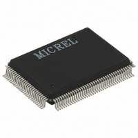
KSZ8995MAI Micrel Inc, KSZ8995MAI Datasheet - Page 13

KSZ8995MAI
Manufacturer Part Number
KSZ8995MAI
Description
IC,Telecom Switching Circuit,CMOS,QFP,128PIN,PLASTIC
Manufacturer
Micrel Inc
Specifications of KSZ8995MAI
Applications
*
Mounting Type
Surface Mount
Package / Case
128-MQFP, 128-PQFP
Number Of Primary Switch Ports
5
Internal Memory Buffer Size
64
Operating Supply Voltage (typ)
Not RequiredV
Fiber Support
Yes
Integrated Led Drivers
Yes
Data Rate
100Mbps
Phy/transceiver Interface
MII/SNI
Power Supply Type
Analog/Digital
Package Type
PQFP
Data Rate (typ)
10/100Mbps
Vlan Support
Yes
Operating Temperature (max)
85C
Operating Temperature (min)
-40C
Pin Count
128
Mounting
Surface Mount
Jtag Support
No
Operating Supply Voltage (max)
Not RequiredV
Operating Supply Voltage (min)
Not RequiredV
Operating Temperature Classification
Industrial
Lead Free Status / RoHS Status
Lead free / RoHS Compliant
For Use With
576-1607 - BOARD EVAL EXPERIMENT KSZ8995MA
Lead Free Status / Rohs Status
Compliant
Other names
576-2126
KSZ8995MAI
KSZ8995MAI
Available stocks
Company
Part Number
Manufacturer
Quantity
Price
Company:
Part Number:
KSZ8995MAI
Manufacturer:
TI
Quantity:
1 700
Company:
Part Number:
KSZ8995MAI
Manufacturer:
MICREL
Quantity:
5
Part Number:
KSZ8995MAI
Manufacturer:
MICREL/麦瑞
Quantity:
20 000
Semptember 2008
Notes:
1.
2.
Pin Number
P = Power supply.
I = Input.
O = Output.
I/O = Bidirectional.
Gnd = Ground.
Ipu = Input w/internal pull-up.
Ipd = Input w/internal pull-down.
Ipd/O = Input w/internal pull-down during reset, output pin otherwise.
Ipu/O = Input w/internal pull-up during reset, output pin otherwise.
NC = No connect.
PU = Strap pin pull-up.
PD = Strap pull-down.
61
62
63
64
65
66
67
68
69
70
71
72
73
74
75
76
77
78
79
80
81
Pin Name
PMRXDV
PMRXER
SMRXDV
PMRXD3
PMRXD2
PMRXD1
PMRXD0
SMTXEN
SMTXER
SMRXD3
SMRXD2
SMTXD3
SMTXD2
SMTXD1
SMTXD0
SMRXC
SMTXC
VDDIO
GNDD
PCRS
PCOL
Type
Ipd/O
Ipd/O
Ipd/O
Ipd/O
Ipd/O
Ipd/O
Ipd/O
Ipd/O
Ipd/O
Ipd/O
Ipd/O
Gnd
Ipd
Ipd
Ipd
Ipd
Ipd
Ipd
I/O
I/O
P
(1)
Port
5
5
5
5
5
5
5
5
Pin Function
PHY[5] MII receive data valid.
PHY[5] MII receive bit 3. Strap option: PD (default) = enable flow control;
PU = disable flow control.
PHY[5] MII receive bit 2. Strap option: PD (default) = disable back
pressure; PU = enable back pressure.
PHY[5] MII receive bit 1. Strap option: PD (default) = drop excessive
collision packets; PU = does not drop excessive collision packets.
PHY[5] MII receive bit 0. Strap option: PD (default) = disable aggressive
back-off algorithm in half-duplex mode; PU = enable for performance
enhancement.
PHY[5] MII receive error. Strap option: PD (default) = packet size
1518/1522 bytes; PU = 1536 bytes.
PHY[5] MII carrier sense/strap option for port 4 only. PD (default) = force
half-duplex if auto-negotiation is disabled or fails. PU = force full-duplex
if auto negotiation is disabled or fails. Refer to Register 76.
PHY[5] MII collision detect/ strap option for port 4 only. PD (default) = no
force flow control, normal operation. PU = force flow control. Refer to
Register 66
Switch MII transmit enable.
Switch MII transmit bit 3.
Switch MII transmit bit 2.
Switch MII transmit bit 1.
Switch MII transmit bit 0.
Switch MII transmit error.
Switch MII transmit clock. Input in MAC mode, output in PHY mode MII.
Digital ground.
3.3V digital V
Switch MII receive clock. Input in MAC mode, output in PHY mode MII.
Switch MII receive data valid.
Switch MII receive bit 3. Strap option: PD (default) = Disable Switch MII
full-duplex flow control; PU = Enable Switch MII full-duplex flow control.
Switch MII receive bit 2. Strap option: PD (default) = Switch MII in full-
duplex mode; PU = Switch MII in half-duplex mode.
13
DD
(2)
for digital I/O circuitry.
M9999-091508


