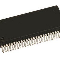
MM908E625ACDWB Freescale Semiconductor, MM908E625ACDWB Datasheet - Page 37

MM908E625ACDWB
Manufacturer Part Number
MM908E625ACDWB
Description
IC QUAD HALF BRDG MCU/LIN 54SOIC
Manufacturer
Freescale Semiconductor
Datasheets
1.MM908E625.pdf
(48 pages)
2.MM908E625ACDWB.pdf
(48 pages)
3.MM908E625ACDWB.pdf
(48 pages)
4.MM908E625ACDWB.pdf
(48 pages)
5.MM908E625ACDWB.pdf
(40 pages)
Specifications of MM908E625ACDWB
Applications
Automotive Mirror Control
Core Processor
HC08
Program Memory Type
FLASH (16 kB)
Controller Series
908E
Ram Size
512 x 8
Interface
SCI, SPI
Number Of I /o
13
Voltage - Supply
8 V ~ 18 V
Operating Temperature
-40°C ~ 85°C
Mounting Type
Surface Mount
Package / Case
54-SOIC (0.300", 7.50mm Width) Exposed Pad
Program Memory Size
16 KB
Number Of Programmable I/os
54
Number Of Timers
16
Operating Supply Voltage
- 18 V to + 28 V
Maximum Operating Temperature
+ 85 C
Mounting Style
SMD/SMT
Minimum Operating Temperature
- 40 C
Lead Free Status / RoHS Status
Contains lead / RoHS non-compliant
Available stocks
Company
Part Number
Manufacturer
Quantity
Price
Company:
Part Number:
MM908E625ACDWB
Manufacturer:
FREESCALE Semiconductor
Quantity:
26
RUN Mode
provides a regulated supply to all digital sections.
parameters (e.g. ICG trim value) are stored in the flash memory
of the device. The following flash memory locations are
reserved for this purpose and might have a value different from
the “empty” (0xFF) state:
mounted onto a thermally enhanced PCB.
MOTOROLA ANALOG INTEGRATED CIRCUIT DEVICE DATA
During RUN mode the main voltage regulator is on. It
To enhance the ease-of-use of the 908E625, various
• 0xFD800xFDDF Trim and Calibration Values
• 0xFFFE:0xFFFF Reset Vector
Figure 21
shows a thermal response curve for a package
Figure 21. Thermal Response of H-Bridge Driver with Package Soldered to a JEDEC PCB Board
5.0
30
25
20
15
10
0.00001 0.0001
5
0
Freescale Semiconductor, Inc.
For More Information On This Product,
FACTORY TRIMMING AND CALIBRATION
0.001
PACKAGE THERMAL PERFORMANCE
Go to: www.freescale.com
0.01
0.1
Time (s)
STOP Mode
regulated output voltage. The STOP mode regulator has a very
limited output current capability. The output voltage will be
lower than the output voltage of the main voltage regulator.
to take care not to erase or override these values. If these
parameters are not used, these flash locations can be erased
and otherwise used.
planes (2s2p). The board conforms to JEDEC EIA/JESD 51-5
and JESD51-7. Substrate thickness is 1.60 mm. Top and
bottom copper trace layers are 0.7 mm thick, with two inner
copper planes of 0.35 mm thickness. Thermal vias have
0.35 mm thick plating.
During STOP mode the STOP mode regulator supplies a
In the event the application uses these parameters, one has
Note The PCB board is a multi-layer with two inner copper
1.0
1
10
100
1000
time[s]
10000
908E625
37


