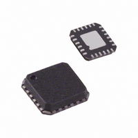
AD8341ACPZ-WP Analog Devices Inc, AD8341ACPZ-WP Datasheet - Page 17

AD8341ACPZ-WP
Manufacturer Part Number
AD8341ACPZ-WP
Description
IC MOD VECT 1.5-2.4GHZ 24LFCSP
Manufacturer
Analog Devices Inc
Datasheet
1.AD8341ACPZ-REEL7.pdf
(20 pages)
Specifications of AD8341ACPZ-WP
Function
Vector, Modulator
Lo Frequency
1.5GHz ~ 2.4GHz
Rf Frequency
1.5GHz ~ 2.4GHz
P1db
8.5dBm
Noise Floor
-150.5dBm/Hz
Current - Supply
145mA
Voltage - Supply
4.75 V ~ 5.25 V
Test Frequency
1.9GHz
Package / Case
24-VFQFN, CSP Exposed Pad
Lead Free Status / RoHS Status
Lead free / RoHS Compliant
EVALUATION BOARD
The evaluation board circuit schematic for the AD8341 is
shown in Figure 41.
The evaluation board is configured to be driven from a
single-ended 50 Ω source. Although the input of the AD8341 is
differential, it may be driven single-ended, with no loss of per-
formance.
The low-pass corner frequency of the baseband I and Q chan-
nels can be reduced by installing capacitors in the C11 and C12
positions. The low-pass corner frequency for either channel is
approximated by
On this evaluation board, the I and Q baseband circuits are
identical to each other, so the following description applies
equally to each. The connections and circuit configuration for
the Q baseband inputs are described in Table 4.
Table 4. Evaluation Board Configuration Options
Components
R7, R9, R11,
R14, R15, R19,
R20, R21, C15,
C19, W3, W4
R1, R3, R10,
R12, R13, R16,
R17, R18, C16,
C20, W1, W2
C11, C12
T1, C17, C18,
L1, L2
L3, L4, C5, C6
f
3dB
≈
45
C
FLT
kHz
+
Function
I Channel Baseband Interface. Resistors R7 and R9 may be installed to accommodate a
baseband source that requires a specific terminating impedance. Capacitors C15 and C19
are bypass capacitors.
For single-ended baseband drive, the Potentiometer R11 can be used to provide a bias level
to the unused input (install either W3 or W4).
Q Channel Baseband Interface. See the I Channel Baseband Interface section.
Baseband Low-Pass Filtering. By adding Capacitor C11 between QFLP and QFLM, and C12
between IFLP and IFLM, the 3 dB low-pass corner frequency of the baseband interface can
be reduced from 230 MHz (nominal). See equation in text.
Output Interface. The 1:1 balun transformer, T1, converts the 50 Ω differential output to 50
Ω single-ended. C17 and C18 are dc blocks. L1 and L2 provide dc bias for the output.
Input Interface. The input impedance of the AD8341 requires 1.2 nH inductors in series
with RFIP and RFIM for optimum return loss when driven by a single-ended 50 Ω line. C5
and C6 are dc blocks.
×
0.5
10
pF
nF
Rev. 0 | Page 17 of 20
The baseband input of the AD8341 requires a differential volt-
age drive. The evaluation board is set up to allow such a drive by
connecting the differential voltage source to QBBP and QBBM.
The common-mode voltage should be maintained at approxi-
mately 0.5 V. For this configuration, Jumpers W1 through W4
should be removed.
The baseband input of the evaluation board may also be driven
with a single-ended voltage. In this case, a bias level is provided
to the unused input from Potentiometer R10 by installing either
W1 or W2.
Setting SW1 in Position B disables the AD8341 output amplifier.
With SW1 set to Position A, the output amplifier is enabled.
With SW1 set to Position A, an external voltage signal, such as a
pulse, can be applied to the DSOP SMA connector to exercise
the output amplifier enable/disable function.
Default Conditions
R7, R9 = Not Installed
R11 = Potentiometer, 2 kΩ,
10 Turn (Bourns)
R14 = 4 kΩ (Size 0603)
R15 = 44 kΩ (Size 0603)
R19, R20, R21 = 0 Ω
(Size 0603)
C15, C19 = 0.1 µF
(Size 0603)
W3 = Jumper (Installed)
W4 = Jumper (Open)
R1, R3 = Not Installed
R10 = Potentiometer, 2 kΩ,
10 Turn (Bourns)
R12 = 4 kΩ (Size 0603)
R13 = 44 kΩ (Size 0603)
R16, R17, R18 = 0 Ω
(Size 0603)
C16, C20 = 0.1 µF
(Size 0603)
W1 = Jumper (Installed)
W2 = Jumper (Open)
C11, C12 = Not Installed
C17, C18 = 100 pF
(Size 0603)
T1 = ETC1-1-13 (M/A-COM)
L1, L2 = 120 nH
(Size 0603)
L3, L4 = 1.2 nH (Size 0402)
C5, C6 = 100 pF (Size 0603)
AD8341


