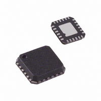
AD8341ACPZ-WP Analog Devices Inc, AD8341ACPZ-WP Datasheet - Page 3

AD8341ACPZ-WP
Manufacturer Part Number
AD8341ACPZ-WP
Description
IC MOD VECT 1.5-2.4GHZ 24LFCSP
Manufacturer
Analog Devices Inc
Datasheet
1.AD8341ACPZ-REEL7.pdf
(20 pages)
Specifications of AD8341ACPZ-WP
Function
Vector, Modulator
Lo Frequency
1.5GHz ~ 2.4GHz
Rf Frequency
1.5GHz ~ 2.4GHz
P1db
8.5dBm
Noise Floor
-150.5dBm/Hz
Current - Supply
145mA
Voltage - Supply
4.75 V ~ 5.25 V
Test Frequency
1.9GHz
Package / Case
24-VFQFN, CSP Exposed Pad
Lead Free Status / RoHS Status
Lead free / RoHS Compliant
SPECIFICATIONS
V
ac-coupled through 1.2 nH series inductor to common, differential-to-single-ended conversion at output using 1:1 balun.
Table 1.
Parameter
OVERALL FUNCTION
RF INPUT STAGE
CARTESIAN CONTROL INTERFACE (I AND Q)
RF OUTPUT STAGE
f = 1.9 GHz
POWER SUPPLY
OUTPUT DISABLE
S
Frequency Range
Maximum Gain
Minimum Gain
Gain Control Range
Phase Control Range
Gain Flatness
Group Delay Flatness
Input Return Loss
Gain Scaling
Modulation Bandwidth
Second Harmonic Distortion
Third Harmonic Distortion
Step Response
Recommended Common-Mode Level
Output Return Loss
Gain
Output Noise Floor
Output IP3
Adjacent Channel Power
Output 1 dB Compression Point
Positive Supply Voltage
Total Supply Current
Disable Threshold
Attenuation
Enable Response Time
Disable Response Time
= 5 V, T
A
= 25°C, Z
O
= 50 Ω, f = 1.9 GHz, single-ended, ac-coupled source drive to RFIP through 1.2 nH series inductor, RFIM
Conditions
Maximum gain setpoint for all phase setpoints
V
(at recommended common-mode level)
Relative to maximum gain
Over 30 dB control range
Over any 60 MHz bandwidth
Over any 60 MHz bandwidth
RFIM, RFIP (Pins 21 and 22)
From RFIP to CMRF (with 1.2 nH series inductors)
IBBP, IBBM, QBBP, QBBM (Pins 16, 15, 3, 4)
500 mV p-p, sinusoidal baseband input single-ended
500 mV p-p, 1 MHz, sinusoidal baseband input differential
500 mV p-p, 1 MHz, sinusoidal baseband input differential
For gain setpoint from 0.1 to 0.9
(V
For gain setpoint from 0.9 to 0.1
(V
RFOP, RFOM (Pins 9, 10)
Measured through balun
Maximum gain setpoint
Maximum gain setpoint, no input
P
f1 = 1900 MHz, f2 = 1897.5 MHz, maximum gain setpoint
CDMA2000, single carrier, P
maximum gain, phase setpoint = 45° (See Figure 35)
Maximum gain
VPS2 (Pins 5, 6, and 14), VPRF (Pins 19 and 24),
RFOP, RFOM (Pins 9 and 10)
Includes load current
DSOP (Pin 13)
(See Figure 24)
DSOP = 5 V
Delay following high-to-low transition until
RF output amplitude is within 10% of final value.
Delay following low-to-high transition until
device produces full attenuation
BBI
IN
BBP
BBP
= 0 dBm, frequency offset = 20 MHz
= V
= 0.5 V, V
= 0.5 V, V
BBQ
= 0 V differential
BBM
BBM
Rev. 0 | Page 3 of 20
= 0.55 V to 0.95 V)
= 0.95 V to 0.55 V)
OUT
= -4 dBm,
Min
1.5
4.75
105
Typ
−4.5
−34.5
30
360
0.5
50
12
2
230
41
47
45
45
0.5
7.5
−4.5
−150.5
−149
17.5
−76
8.5
5
125
V
33
30
15
s
/2
Max
2.4
5.25
145
AD8341
Unit
GHz
dB
dB
dB
Degrees
dB
ps
dB
1/V
MHz
dBc
dBc
ns
ns
V
dB
dB
dBm/Hz
dBm/Hz
dBm
dBm
dBm
V
mA
V
dB
ns
ns


