ADNS-2610 Avago Technologies US Inc., ADNS-2610 Datasheet - Page 13
ADNS-2610
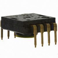
Manufacturer Part Number
ADNS-2610
Description
SENSOR OPTICAL MOUSE 8-DIP
Manufacturer
Avago Technologies US Inc.
Datasheet
1.ADNK-2610.pdf
(27 pages)
Specifications of ADNS-2610
Lead Free Status / RoHS Status
Lead free / RoHS Compliant
Lead Free Status / RoHS Status
Lead free / RoHS Compliant, Lead free / RoHS Compliant
Other names
516-1843
ADNS-2610
ADNS-2610


Read Operation
A read operation, meaning data that is going from the
ADNS-2610 to the microcontroller, is always initiated by
the microcontroller and consists of two bytes. The first
byte that contains the address is written by the microcon-
troller and has a “0” as its MSB to indicate data direction.
The second byte contains the data and is driven by the
ADNS-2610. The transfer is synchronized by SCK. SDIO is
Figure 21. Read operation.
Detail "A"
Microcontroller
to ADNS-2610
SDIO handoff
Figure 22. Microcontroller to ADNS-2610 SDIO handoff.
Detail "B"
ADNS-2610 to
Microcontroller
SDIO handoff
Figure 2. ADNS-2610 to microcontroller SDIO handoff.
NOTE:
The 250 ns high state of SCK is the minimum data hold time of the ADNS-
2610. Since the falling edge of SCK is actually the start of the next read
or write command, the ADNS-2610 will hold the state of D
line until the falling edge of SCK. In both write and read operations, SCK
is driven by the microcontroller.
1
Cycle #
SDIO
SCK
SCK
1
SDIO
0
SCK
SDIO
SCK
Released by ADNS-2610
A
2
6
A
1
A
SDIO Driven by Microcontroller
3
5
D
0
4
A
4
60 ns, min
5
A
3
250 ns, min
R/W bit of next address
6
A
160 ns, max
2
Driven by microcontroller
0
250 ns, min
on the SDIO
A
0
7
A
1
100 µs, min
t
HOLD
A
0
8
Detail "A"
0 ns, min
changed on falling edges of SCK and read on every rising
edge of SCK. The microcontroller must go to a High-Z
state after the last address data bit. The ADNS-2610 will
go to the High-Z state after the last data bit. Another
thing to note during a read operation; SCK needs to be
delayed after the last address data bit to ensure that the
ADNS-2610 has at least 100 µs to prepare the requested
data. This is shown in the timing diagrams below (See
Figures 21 to 23).
D
9
7
10
D
6
Hi-Z
11
D
250 ns, max
5
SDIO Driven by ADNS-2610
12
D
160 ns, min
D
4
7
13
D
3
D
6
250 ns, max
14
D
2
15
D
1
16
D
Detail "B"
0
Related parts for ADNS-2610
Image
Part Number
Description
Manufacturer
Datasheet
Request
R

Part Number:
Description:
Optical Mouse Sensor,DIP
Manufacturer:
Avago Technologies US Inc.
Datasheet:

Part Number:
Description:
Optical Mouse Sensor,DIP
Manufacturer:
Avago Technologies US Inc.
Datasheet:

Part Number:
Description:
Trim Lens For ADNS-3530
Manufacturer:
Avago Technologies US Inc.
Datasheet:

Part Number:
Description:
8 DIP SFF Navigation Sensor
Manufacturer:
Avago Technologies US Inc.
Datasheet:

Part Number:
Description:
Trim Lens For ADNS-5090
Manufacturer:
Avago Technologies US Inc.
Datasheet:

Part Number:
Description:
BLACK CLIP FOR ADNS-5000
Manufacturer:
Avago Technologies US Inc.
Datasheet:
Part Number:
Description:
Lens For ADNS-7630
Manufacturer:
Avago Technologies US Inc.
Datasheet:

Part Number:
Description:
Optical Mouse Sensor,DIP
Manufacturer:
Avago Technologies US Inc.
Datasheet:
Part Number:
Description:
Optical Mouse Sensor,DIP
Manufacturer:
Avago Technologies US Inc.
Datasheet:
Part Number:
Description:
Low Power Wireless LED Sensor
Manufacturer:
Avago Technologies US Inc.
Datasheet:

Part Number:
Description:
OPTOCOUPLER GATE DRV 2A 16-SOIC
Manufacturer:
Avago Technologies US Inc.
Datasheet:
Part Number:
Description:
OPTOCOUPLER 2CH 2.5A 16-SOIC
Manufacturer:
Avago Technologies US Inc.
Datasheet:

Part Number:
Description:
OPTOCOUPLER GATE DRV 0.4A 16SOIC
Manufacturer:
Avago Technologies US Inc.
Datasheet:

Part Number:
Description:
OPTOCOUPLER 2.0A 250KHZ 8-DIP
Manufacturer:
Avago Technologies US Inc.
Datasheet:

Part Number:
Description:
OPTOCOUPLER 2.0A 250KHZ GW 8-SMD
Manufacturer:
Avago Technologies US Inc.
Datasheet: