PMEG4010ET T/R NXP Semiconductors, PMEG4010ET T/R Datasheet
PMEG4010ET T/R
Specifications of PMEG4010ET T/R


Related parts for PMEG4010ET T/R


PMEG4010ET T/R Summary of contents
Page 1
PMEG4010EH; PMEG4010EJ; PMEG4010ET 1 A very low V Rev. 04 — 21 March 2007 1. Product profile 1.1 General description Planar Maximum Efficiency General Application (MEGA) Schottky barrier rectifiers with an integrated guard ring for stress protection, encapsulated in small ...
Page 2
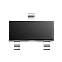
... NXP Semiconductors 2. Pinning information Table 3. Pin SOD123F; SOD323F 1 2 SOT23 [1] The marking bar indicates the cathode. 3. Ordering information Table 4. Type number PMEG4010EH PMEG4010EJ PMEG4010ET 4. Marking Table 5. Type number PMEG4010EH PMEG4010EJ PMEG4010ET [ made in Hong Kong * = p: made in Hong Kong * = t: made in Malaysia * = W: made in China ...
Page 3
... NXP Semiconductors 5. Limiting values Table 6. In accordance with the Absolute Maximum Rating System (IEC 60134). Symbol FRM I FSM P tot amb T stg [1] Device mounted on an FR4 Printed-Circuit Board (PCB), single-sided copper, tin-plated and standard footprint. [2] Device mounted on an FR4 PCB, single-sided copper, tin-plated, mounting pad for cathode 1 cm [3] Refl ...
Page 4
... NXP Semiconductors 6. Thermal characteristics Table 7. Symbol R th(j-a) R th(j-sp) [1] For Schottky barrier diodes thermal runaway has to be considered some applications the reverse power losses P [2] Device mounted on an FR4 PCB, single-sided copper, tin-plated and standard footprint. [3] Device mounted on an FR4 PCB, single-sided copper, tin-plated, mounting pad for cathode 1 cm [4] Refl ...
Page 5
... NXP Semiconductors (mA (1) (2) (3) (4) ( 0.1 0.2 0.3 ( 150 C amb ( 125 C amb ( amb ( amb ( amb Fig 1. Forward current as a function of forward voltage; typical values MHz amb Fig 3. Diode capacitance as a function of reverse voltage; typical values PMEG4010EH_EJ_ET_4 Product data sheet 1 A very low V ...
Page 6
... NXP Semiconductors 8. Test information Fig 4. Duty cycle definition 9. Package outline 1.7 1.5 1 3.6 2.7 3.4 2.5 2 0.70 0.55 Dimensions in mm Fig 5. Package outline SOD123F Fig 7. Package outline SOT23 (TO-236AB) PMEG4010EH_EJ_ET_4 Product data sheet 1 A very low 1.2 1.0 0.55 0.35 0.25 ...
Page 7
... NXP Semiconductors 10. Packing information Table 9. The indicated -xxx are the last three digits of the 12NC ordering code. Type number PMEG4010EH PMEG4010EJ PMEG4010ET [1] For further information and the availability of packing methods, see 11. Soldering Fig 8. Reflow soldering footprint SOD123F Fig 9. Reflow soldering footprint SOD323F (SC-90) ...
Page 8
... NXP Semiconductors Fig 10. Reflow soldering footprint SOT23 (TO-236AB) 4.60 Fig 11. Wave soldering footprint SOT23 (TO-236AB) PMEG4010EH_EJ_ET_4 Product data sheet 1 A very low V 2.90 2.50 0.85 2 3.00 1.30 0.85 3 0.50 (3x) 0.60 (3x) 1.00 3.30 3.40 1.20 (2x 4.00 1.20 3 2.80 4.50 Rev. 04 — 21 March 2007 PMEG4010EH/EJ/ET MEGA Schottky barrier rectifi ...
Page 9
... Data sheet status Product data sheet The format of this data sheet has been redesigned to comply with the new identity guidelines of NXP Semiconductors. Legal texts have been adapted to the new company name where appropriate. Type numbers PMEG4010EH and PMEG4010EJ separated from data sheet ...
Page 10
... For detailed and full information see the relevant full data sheet, which is available on request via the local NXP Semiconductors sales office. In case of any inconsistency or conflict with the short data sheet, the full data sheet shall prevail ...
Page 11
... NXP Semiconductors 15. Contents 1 Product profi 1.1 General description 1.2 Features . . . . . . . . . . . . . . . . . . . . . . . . . . . . . . 1 1.3 Applications . . . . . . . . . . . . . . . . . . . . . . . . . . . 1 1.4 Quick reference data Pinning information . . . . . . . . . . . . . . . . . . . . . . 2 3 Ordering information . . . . . . . . . . . . . . . . . . . . . 2 4 Marking . . . . . . . . . . . . . . . . . . . . . . . . . . . . . . . . 2 5 Limiting values Thermal characteristics Characteristics . . . . . . . . . . . . . . . . . . . . . . . . . . 4 8 Test information . . . . . . . . . . . . . . . . . . . . . . . . . 6 9 Package outline . . . . . . . . . . . . . . . . . . . . . . . . . 6 10 Packing information Soldering . . . . . . . . . . . . . . . . . . . . . . . . . . . . . . 7 12 Revision history ...