BAS56,235 NXP Semiconductors, BAS56,235 Datasheet - Page 8
BAS56,235
Manufacturer Part Number
BAS56,235
Description
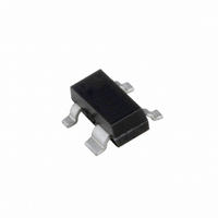
DIODE DUAL SW 120V 200MA SOT143
Manufacturer
NXP Semiconductors
Datasheet
1.BAS56215.pdf
(12 pages)
Specifications of BAS56,235
Package / Case
SOT-143, SOT-143B, TO-253AA
Voltage - Forward (vf) (max) @ If
1V @ 200mA
Current - Reverse Leakage @ Vr
100nA @ 120V
Current - Average Rectified (io) (per Diode)
200mA (DC)
Voltage - Dc Reverse (vr) (max)
60V
Reverse Recovery Time (trr)
6ns
Diode Type
Standard
Speed
Small Signal =< 200mA (Io), Any Speed
Diode Configuration
2 Independent
Mounting Type
Surface Mount
Product
Switching Diodes
Peak Reverse Voltage
60 V
Forward Continuous Current
0.2 A
Max Surge Current
9 A
Configuration
Dual Parallel
Recovery Time
6 ns
Forward Voltage Drop
1 V
Maximum Reverse Leakage Current
0.1 uA
Operating Temperature Range
+ 150 C
Maximum Operating Temperature
+ 150 C
Minimum Operating Temperature
- 65 C
Mounting Style
SMD/SMT
Lead Free Status / RoHS Status
Lead free / RoHS Compliant
Lead Free Status / RoHS Status
Lead free / RoHS Compliant, Lead free / RoHS Compliant
Other names
933742310235
BAS56 /T3
BAS56 /T3
BAS56 /T3
BAS56 /T3


NXP Semiconductors
11. Soldering
BAS56
Product data sheet
Fig 9.
Fig 10. Wave soldering footprint BAS56 (SOT143B)
4.6
(3×)
0.7
0.7
2.575
Reflow soldering footprint BAS56 (SOT143B)
(3×)
0.6
0.6
All information provided in this document is subject to legal disclaimers.
0.75
(3×)
(3×)
0.6
0.5
0.9
1
Rev. 3 — 29 June 2010
3.25
1.9
4.45
2.2
1.2
0.95
(3×)
1.2
1
2
3
1.425
1.425
(3×)
preferred transport direction during soldering
High-speed double diode
Dimensions in mm
Dimensions in mm
© NXP B.V. 2010. All rights reserved.
solder lands
solder resist
solder paste
occupied area
BAS56
solder lands
solder resist
occupied area
sot143b_fr
sot143b_fw
8 of 12
Related parts for BAS56,235
Image
Part Number
Description
Manufacturer
Datasheet
Request
R

Part Number:
Description:
The BAS56 consists of two high-speedswitching diodes fabricated inplanar technology, and encapsulatedin the small rectangular plastic SMDSOT143 package
Manufacturer:
NXP Semiconductors
Datasheet:

Part Number:
Description:
Diodes (General Purpose, Power, Switching) DIODE SW TAPE-11
Manufacturer:
NXP Semiconductors

Part Number:
Description:
DIODE SW 60V 200MA HS SOT143B
Manufacturer:
NXP Semiconductors
Datasheet:

Part Number:
Description:
DIODE SCHOTTKY DUAL 70V SOT-23
Manufacturer:
Infineon Technologies
Datasheet:

Part Number:
Description:
DIODE SW 80V 200MA HS SOT143
Manufacturer:
Infineon Technologies
Datasheet:

Part Number:
Description:
DIODE SW GP 80V 200MA SOT-363
Manufacturer:
Infineon Technologies
Datasheet:

Part Number:
Description:
DIODE SCHOTTKY 70V CA SOT-23
Manufacturer:
Infineon Technologies

Part Number:
Description:
DIODE SW HS 200V 250MA SC-74
Manufacturer:
Infineon Technologies

Part Number:
Description:
DIODE SCHOTTKY 70V SER SOT-323
Manufacturer:
Infineon Technologies
Part Number:
Description:
DIODE SCHOTTKY 40V SOT-23
Manufacturer:
Infineon Technologies
Datasheet:
Part Number:
Description:
DIODE SCHOTTKY DUAL 70V SOT-23
Manufacturer:
Infineon Technologies
Part Number:
Description:
DIODE SCHOTTKY 40V SOT-23
Manufacturer:
Infineon Technologies
Datasheet:

Part Number:
Description:
DIODE SCHTKY CC 40V 120MA SOT-23
Manufacturer:
Infineon Technologies
Datasheet:

Part Number:
Description:
DIODE SCHOTTKY CA 70V 70MA SOT23
Manufacturer:
Infineon Technologies

Part Number:
Description:
DIODE SCHOTTKY CC 70V 70MA SOT23
Manufacturer:
Infineon Technologies