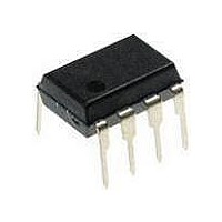
TISP61512P-S Bourns Inc., TISP61512P-S Datasheet - Page 6

TISP61512P-S
Manufacturer Part Number
TISP61512P-S
Description
Sidacs
Manufacturer
Bourns Inc.
Datasheet
1.TISP61512P-S.pdf
(9 pages)
Specifications of TISP61512P-S
Breakover Current Ibo Max
5 A
Rated Repetitive Off-state Voltage Vdrm
100 V
Off-state Leakage Current @ Vdrm Idrm
0.005 mA
Forward Voltage Drop
4 V
Mounting Style
Through Hole
Package / Case
PDIP-8
Lead Free Status / RoHS Status
Lead free / RoHS Compliant
Thyristor based overvoltage protectors, for telecommunications equipment, became popular in the late 1970s. These were fixed voltage
breakover triggered devices, likened to solid state gas discharge tubes. As these were new forms of thyristors, the existing thyristor terminology
did not cover their special characteristics. This resulted in the invention of new terms based on the application usage and device characteristic.
Initially, there was a wide diversity of terms to describe the same thing, but today the number of terms have reduced and stabilized.
Programmable, (gated), overvoltage protectors are relatively new and require additional parameters to specify their operation. Similarly to the
fixed voltage protectors, the introduction of these devices has resulted in a wide diversity of terms to describe the same thing. To help promote
an understanding of the terms and their alternatives, this section has a list of alternative terms and the parameter definitions used for this data
sheet. In general, the Bourns approach is to use terms related to the device internal structure, rather than its application usage as a single
device may have many applications each using a different terminology for circuit connection.
This guide is intended to help the translation of alternative symbols to those used in this data sheet. As in some cases the alternative symbols
have no substance in international standards and are not fully defined by the originators, users must confirm symbol equivalence. No liability
will be assumed from the use of this guide.
General
Alternative Symbol Cross-Reference Guide
Non-repetitive peak on -state pulse current
Off-state current
Gate reverse current (with A and K terminals connected)
Off-state voltage
Peak forward recovery voltage
Breakover voltage
Gate voltage, (V
to the A terminal)
Repetitive peak off-state voltage
Repetitive peak gate-cathode voltage
Gate-cathode voltage
Gate-cathode voltage at breakover
Cathode-anode voltage
Anode-cathode capacitance
Cathode 1 terminal
Cathode 2 terminal
Anode terminal
Gate terminal
Thermal Resistance, junction to ambient
TISP61511D Gated Protectors
GG
is gate supply voltage referenced
Parameter
DEVICE PARAMETERS
Data Sheet
Symbol
V
V
V
V
V
GK(BO)
R
I
I
V
C
GAS
TSP
V
V
DRM
GKM
K1
K2
FRM
V
(BO)
I
G
A
θJA
GK
D
AK
G
D
K
Al ternative
V
Symbol
R
GND/LINE
Customers should verify actual device performance in their specific applications.
V
V
V
V
V
GND
Gate
V
Ring
th
V
V
I
V
I
GATE
V
C
Tip
I
V
V
MLG
MGL
RM
RG
SGL
gate
PP
I
RM
DGL
FP
LG
R
GL
R
S
off
(j-a)
Peak pulse current
Reverse leakage current LINE/GND
Reverse leakage current GATE/LINE
Reverse voltage LINE/GND
Peak forward voltage LINE/GND
Dynamic switching voltage GND/LINE
GATE/GND voltage
Maximum voltage LINE/GND
Maximum voltage GATE/LINE
GATE/LINE voltage
Dynamic switching voltage GATE/LINE
LINE/GND voltage
Off-state capacitance LINE/GND
Tip terminal
Ring terminal
Ground terminal
Gate terminal
Thermal Resistance, junction to ambient
Alternative Parameter
Specifications are subject to change without notice.
JULY 1995 — REVISED JULY 2008


