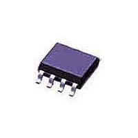
TISPPBL1DR Bourns Inc., TISPPBL1DR Datasheet - Page 10

TISPPBL1DR
Manufacturer Part Number
TISPPBL1DR
Description
Sidacs SURGE SUP 8-SOP
Manufacturer
Bourns Inc.
Datasheet
1.TISPPBL3SE.pdf
(18 pages)
Specifications of TISPPBL1DR
Mounting Style
SMD/SMT
Package / Case
SO-8
Lead Free Status / RoHS Status
Lead free / RoHS Compliant
Available stocks
Company
Part Number
Manufacturer
Quantity
Price
Company:
Part Number:
TISPPBL1DR
Manufacturer:
STM
Quantity:
21 600
Part Number:
TISPPBL1DR
Manufacturer:
TI/德州仪器
Quantity:
20 000
TISPPBL1D, TISPPBL1P, TISPPBL2D, TISPPBL2P
DUAL FORWARD-CONDUCTING P-GATE THYRISTORS
FOR ERICSSON COMPONENTS SLICS
limiting voltage levels
SLIC protection requirements
temperature range
10
di/dt is about 50 A/µs.
Fifty devices were measured in the test circuit of Figure 3. The 50 devices were made up from groups of 5
devices taken from 10 separately processed device lots. Figure 7 shows the total waveform variation of the
thyristor limiting voltage across the 50 devices. This shows that the largest peak limiting voltage (Breakover
voltage, V
exceeds the gate reference supply voltage level for a period (t
Figure 9 and Figure 11 show these two waveform parameters in terms of device population. In Figure 9, the
limiting voltage is shown in terms of the overshoot beyond the gate reference supply (V
the gate reference voltage level magnifies the thyristor limiting voltage variation and shows the data
stratification caused by the oscilloscope digitisation. Extrapolating the data trend indicates that the overshoot
is less than 14 V at the 99.997% level (equal to 30 ppm of the population exceeding 14 V, equivalent to +4
sigma point of a normal distribution). In Figure 11, extrapolating the thyristor data trend to the 99.997% level
indicates a maximum breakdown time, t
85 °C increases the thyristor peak limiting voltage by 2.4%, giving a maximum 85 °C peak limiting voltage of
1.024x(-50-14) = -65.5 V. Over the -40 °C to 85 °C temperature range the TISPPBLx is specified to have a
maximum V
Figure 8 shows the total waveform variation of the diode limiting voltage across the 50 devices. The peak
limiting voltage (Peak Forward Recovery Voltage V
magnetically induced noise in the probe. Figure 9 shows that extrapolated 99.997% level is about 5.5 V. In
Figure 11, extrapolating the diode data trend to the 99.997% level indicates a maximum forward recovery
time, t
recovery time of 1 µs.
Diodes do not switch to a much lower voltage like thyristors, so the diode limiting voltage applies for the whole
impulse duration. Forward voltages of 1 V or less are normally considered safe. Figure 10 shows that the
lowest current 1 V condition occurs at -40 °C with a current of 0.3 A. When the TISPPBLx is tested with the
rated 10/1000 impulse it would take about 8 ms for the current to decay from 30 A to 0.3 A. Over the -40 °C to
85 °C temperature range, the TISPPBLx is specified to have a V
at 60 A/µs, this rate then reduces as the peak current is approached. At the TISPPBLx V
85 °C. This gives a maximum 85 °C peak limiting voltage of 1.1x(5.5) = 6.1 V. Over the -40 °C to 85 °C
temperature range, the TISPPBLx is specified to have a maximum V
This clause discusses the voltage withstand capabilities of the various Ericsson Components SLIC groups
and compares these to the TISPPBLx protector parameters. The examples provided are intended to provide
designers information on how the TISPPBLx protector and specific SLICs work together. Designers should
always follow the circuit design recommendations contained in the latest edition of a SLIC data sheet.
Some SLICs are rated for 0 °C to 70 °C operation, others for -40 °C to 85 °C operation. The TISPPBLx
protector is specified for -40 °C to 85 °C operation and so covers both temperature ranges.
FR
, of 0.1 µs. Figure 12 indicates that there is about a 10% uplift by increasing the temperature to
(BO)
(BO)
) is -62 V, a 12 V overshoot beyond the -50 V gate reference supply, V
value of -70 V and a breakdown time, t
(BR)
, of 0.5 µs. Figure 12 shows that increasing the temperature up to
FRM
(BR)
) is less than 6 V, and this value includes the 2 V of
P R O D U C T
, of 1 µs.
(BR)
F
) of about 0.4 µs.
below 1 V within 10 ms.
FRM
Specifications are subject to change without notice.
value of 8 V and a maximum forward
AUGUST 1997 - REVISED AUGUST 2002
I N F O R M A T I O N
B
. The limiting voltage
B
(BO)
- V
(BO)
condition the
). Removing


